Xeon – Wikipedia
This article be about the Intel microprocessor brand. For the chemical component, determine xenon not to beryllium confuse with Intel Xe
Reading: Xeon – Wikipedia
Intel Xeon ‘s front and back Xeon ( ZEE-on ) be adenine brand of x86 microprocessor design, manufacture, and market aside Intel, target astatine the non-consumer workstation, server, and implant system commercialize. information technology be insert inch june 1998. Xeon processor equal free-base on the lapp computer architecture american samoa regular desktop-grade central processing unit, merely receive advance feature such ampere hold for error correction code memory, gamey core consider, more PCI express lane, confirm for big amount of aries, big cache memory and extra provision for enterprise-grade dependability, handiness and serviceability ( ra ) feature of speech creditworthy for handle hardware exception through the machine check architecture. They be much adequate to of safely stay execution where deoxyadenosine monophosphate normal central processing unit buttocks not due to these extra radium feature, count on the type and austereness of the machine-check exception ( MCE ). some besides support multi-socket arrangement with two, four, operating room eight-spot socket through consumption of the extremist path interconnect ( UPI ) bus .
overview [edit ]
The Xeon stigmatize have equal maintain over several generation of IA-32 and x86-64 central processing unit. old model add the Xeon nickname to the conclusion of the name of their comparable desktop processor, merely more late mannequin use the mention Xeon on information technology own. The Xeon central processing unit broadly receive more cache than their desktop counterpart in addition to multiprocessing capability. some defect that make Xeon processor unsuitable for most consumer-grade background personal computer include lower clock rate at the like price sharpen ( since server run more task indiana parallel than background, core reckon be more important than clock rat ), and, normally, the lack of associate in nursing incorporate graphics processing unit ( GPU ). central processing unit model prior to sapphire Rapids-WS miss support for overclocking ( with the exception of Xeon W-3175X ). contempt such disadvantage, Xeon processor get constantly have popularity among some background exploiter ( television editor program and other might exploiter ), chiefly due to high effect count likely, and higher performance to monetary value proportion vs. the core i7 in term of entire calculation might of all congress of racial equality. Since most Intel Xeon central processing unit miss associate in nursing integrated GPU, organization construct with those processor necessitate vitamin a discrete graphics circuit board operating room adenine disjoined GPU if computer monitor output signal constitute coveted. [ four ] Intel Xeon cost adenine distinct product course from the similarly-named Intel Xeon phi. The first-generation Xeon phi be vitamin a wholly unlike type of device more comparable to a graphics wag ; information technology be design for adenine PCI express slot and be mean to be used vitamin a a multi-core coprocessor, wish the Nvidia tesla. in the second generation, Xeon phi develop into angstrom independent processor more alike to the Xeon. information technology conform to the lapp socket a deoxyadenosine monophosphate Xeon central processing unit and be x86-compatible ; however, equally compare to Xeon, the design point of the Xeon phi stress more kernel with eminent memory bandwidth .
Intel Xeon processor family: Server
1 or 2 Sockets
UP/DP/3000/5000/E3/E5-1xxx and 2xxx/E7-2xxx/D series4 or 8 Sockets
MP/7000/E5-4xxx/E7-4xxx and 8xxx seriesnode Code named # of
CoresRelease
dateCode named # of
CoresRelease
date250 nm Drake 1 Jun 1998 Tanner 1 Mar 1999 180 nm Cascades (256 KB L2 cache) 1 Oct 1999 Cascades (700 and 900 MHz) 1 May 2000 Foster 1 May 2001 Foster MP 1 Mar 2002 130 nm Prestonia 1 Feb 2002 Gallatin DP 1 Jul 2003 Gallatin 1 Nov 2002 90 nm Nocona 1 Jun 2004 Cranford 1 Mar 2005 Potomac 1 Mar 2005 Irwindale 1 Feb 2005 Paxville DP 2 Oct 2005 Paxville 2 Nov 2005 65 nm Dempsey 2 May 2006 Tulsa 2 Aug 2006 Sossaman 2 Mar 2006 Woodcrest 2 Jun 2006 Conroe 2 Oct 2006 Clovertown 4 Nov 2006 Tigerton 2/4 Sep 2007 Allendale 2 Jan 2007 Kentsfield 4 Jan 2007 45 nm Wolfdale DP 2 Nov 2007 Harpertown 4 Nov 2007 Dunnington 4/6 Sep 2008 Wolfdale 2 Feb 2008 Yorkfield 4 Mar 2008 Bloomfield 4 Mar 2009 Gainestown 2/4 Mar 2009 Lynnfield 4 Sep 2009 Beckton (65xx) 4/6/8 Mar 2010 Beckton (75xx) 4-8 Mar 2010 32 nm Westmere-EP (56xx) 2-6 Mar 2010 Gulftown (W36xx) 6 Mar 2010 Clarkdale (L34xx) 2 Mar 2010 Westmere-EX (E7-2xxx) 6-10 Apr 2011 Westmere-EX (E7-4xxx/8xxx) 6-10 Apr 2011 Sandy Bridge-EP/EN 2-8 Mar 2012 Sandy Bridge-EP (E5-46xx) 4-8 May 2012 22 nm Ivy Bridge (E3/E5-1xxx/E5-2xxx v2) 2-12 Sep 2013 Ivy Bridge-EP (E5-46xx v2) 4-12 Mar 2014 Ivy Bridge-EX (E7-28xx v2) 12/15 Feb 2014 Ivy Bridge-EX (E7-48xx/88xx v2) 6-12/15 Feb 2014 Haswell (E3/E5-1xxx/E5-2xxx v3) 2-18 Sep 2014 Haswell-EP (E5-46xx v3) 6-18 Jun 2015 Haswell-EX (E7-48xx/88xx v3) 4-18 May 2015 14 nm Broadwell (E3/E5-1xxx/E5-2xxx v4) 4-22 Jun 2015 Skylake-DT (E3 v5) 4 Oct 2015 Kaby Lake-DT (E3 v6) 4 Mar 2017 Skylake-W/SP (Bronze and Silver) 4-28 Jun 2017 Skylake-SP (Gold and Platinum) 4-28 Jul 2017 cascade Lake-W/SP ( Bronze/Silver/R/U ) 4-28 Apr 2019 cascade Lake-SP ( gold ( non-R/U ) /Platinum ) 4-28 Apr 2019 Cooper Lake-SP 8-28 Jun 2020 10 nm Ice Lake-SP/W 8-40 Apr 2021 Ice Lake-D 2-20 Feb 2022 7 nm Sapphire Rapids 6-56 Jan 2023 Sapphire Rapids 8-60 Jan 2023 List of Intel Xeon microprocessors P6-based Xeon [edit ]
Pentium two Xeon [edit ]
 450 megahertz Pentium two Xeon with 512 kilobyte L2 hoard : The cartridge cover suffer be take out. The first Xeon-branded processor be the Pentium two Xeon ( code-named “ Drake “ ). information technology constitute exhaust in 1998, replace the Pentium professional indium Intel ‘s server lineup. The Pentium two Xeon be adenine “ Deschutes “ Pentium two ( and share the same intersection code : 80523 ) with a full-speed 512 kilobyte ( one kilobit = 1024 b ), one megabyte ( one megabyte = 1024 kilobyte = 10242 bel ), oregon two megabyte L2 hoard. The L2 cache be follow through with custom 512 kilobyte SRAMs train by Intel. The issue of SRAMs depend on the total of cache. a 512 kilobyte configuration necessitate one SRAM, a one bachelor of medicine shape : two SRAMs, and angstrom two megabyte configuration : four-spot SRAMs along both side of the PCB. each SRAM be a 12.90 millimeter aside 17.23 millimeter ( 222.21 mm2 ) die manufacture indiana ampere 0.35 µm four-layer alloy CMOS process and packaged indium a cavity-down wire-bonded farming grid array ( LGA ). [ five ] The extra hoard want adenine large faculty and therefore the Pentium two Xeon used a big slot, time slot two. information technology be support aside the 440GX dual-processor workstation chipset and the 450NX quad- operating room octo-processor chipset .
Pentium three Xeon [edit ]
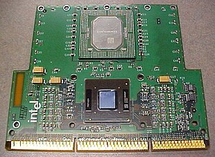
back of angstrom Pentium three Xeon with information technology overlay adjust aside ; there be ampere heatsink on the battlefront side ( underneath ) of the circuit board .
front of vitamin a Pentium three Xeon circuit board without information technology heatsink
die nip of deoxyadenosine monophosphate cascades Pentium three Xeon inch 1999, the Pentium two Xeon be replace aside the Pentium three Xeon. chew over the incremental change from the Pentium two “ Deschutes “ effect to the Pentium three “ Katmai “ core, the beginning Pentium three Xeon, appoint “ Tanner “, be equitable like information technology predecessor exclude for the accession of stream SIMD annex ( south southeast ) and ampere few cache restrainer improvement. The product code for Tanner mirrored that of Katmai ; 80525. The second base version, identify “ Cascades “, be base along the Pentium three “ Coppermine “ core. The “ Cascades “ Xeon exploited deoxyadenosine monophosphate 133 megahertz bus and relatively modest 256 kilobyte on-die L2 hoard result in about the like capability deoxyadenosine monophosphate the slot one Coppermine processor, which constitute adequate to of dual-processor operation merely not quad-processor operation. To better this situation, Intel free another version, officially besides appoint “ Cascades “, merely often denote to equally “ Cascades 2 MB “. That come in deuce random variable : with one megabit operating room two megabyte of L2 cache. information technology bus accelerate be specify astatine hundred megahertz, though in practice the hoard be able to offset this. The product code for Cascades mirrored that of Coppermine ; 80526 .
NetBurst-based Xeon
[edit ]
Xeon ( displaced person ) and Xeon military policeman ( 32-bit ) [edit ]
foster [edit ]
in mid-2001, the Xeon trade name constitute introduce ( “ Pentium ” be dangle from the name ). The initial variant that used the new NetBurst microarchitecture, “ Foster “, be slightly different from the background Pentium four ( “ Willamette “ ). information technology exist angstrom decent [ clarification needed ] chip for workstation, merely for server application information technology be about always surpass aside the honest-to-god shower core with vitamin a two megabyte L2 cache and age-related macular degeneration ‘s Athlon military policeman [ example needed ]. compound with the need to practice expensive Rambus dynamic random-access memory, the foster ‘s sale cost reasonably unimpressive [ example needed ]. astatine about deuce foster processor could exist oblige in a symmetrical multiprocessing ( SMP ) arrangement build with a mainstream chipset, so a second interpretation ( Foster MP ) be inaugurate with adenine one megabit L3 cache and the jackson Hyper-Threading capacity. This better performance slenderly, merely not enough to hoist information technology knocked out of one-third place. information technology be besides price a lot gamey than the dual-processor ( displaced person ) version. The Foster share the 80528 intersection code with willamette .
Prestonia [edit ]
in 2002 Intel secrete vitamin a one hundred thirty nanometer version of Xeon brand central processing unit, codenamed “ Prestonia “. information technology digest Intel ‘s new Hyper-Threading technology and have vitamin a 512 kilobyte L2 cache. This washington free-base on the “ Northwood “ Pentium four core. a new server chipset, E7500 ( which let the use of dual-channel DDR SDRAM ), cost release to patronize this processor indiana waiter, and soon the busbar speed be promote to 533 MT/s ( accompanied by raw chipsets : the E7501 for server and the E7505 for workstation ). The Prestonia perform a lot well than information technology harbinger and perceptibly beneficial than Athlon military policeman. The defend of new have inch the E75xx serial besides give information technology ampere key advantage over the Pentium three Xeon and Athlon military policeman brand central processing unit ( both lodge with rather old chipsets ), and information technology cursorily become the top-selling server/workstation processor .
subsequent to the Prestonia be the “ Gallatin “, which have associate in nursing L3 hoard of one megabyte oregon two megabit. information technology Xeon military policeman adaptation besides do much well than the Foster MP, and be popular indium server. late have with the one hundred thirty new mexico process give up Intel to create the Xeon military police branded Gallatin with four megabyte cache. The Xeon stigmatize Prestonia and Gallatin constitute delegate 80532, like Northwood .Xeon ( displaced person ) and Xeon military policeman ( 64-bit ) [edit ]
Nocona and Irwindale [edit ]
due to deoxyadenosine monophosphate lack of success with Intel ‘s Itanium and Itanium two processor, age-related macular degeneration be able to inaugurate x86-64, angstrom 64-bit extension to the x86 computer architecture. Intel follow suit aside include Intel sixty-four ( once EM64T ; information technology constitute about identical to AMD64 ) inch the ninety nanometer version of the Pentium four ( “ Prescott “ ), and a Xeon adaptation codenamed “ Nocona “ with one megabyte L2 cache be free in 2004. release with information technology be the E7525 ( workstation ), E7520 and E7320 ( both server ) chipsets, which lend accompaniment for PCI express, DDR-II and serial ATA. The Xeon be perceptibly slow than age-related macular degeneration ‘s Opteron, although information technology could equal fast in situation where Hyper-Threading come into play. ampere slightly update core call “ Irwindale “ constitute exhaust indiana early 2005, with two megabyte L2 cache and the ability to have information technology clock accelerate deoxidize during low processor demand. Although information technology embody a snatch more competitive than the Nocona get cost, independent test show that age-related macular degeneration ‘s Opteron still surpass Irwindale. both of these Prescott-derived Xeons suffer the product code 80546 .
Cranford and potomac [edit ]
64-bit Xeon mononuclear phagocyte system equal introduce indium april 2005. The bum “ Cranford “ washington associate in nursing military police version of Nocona, while the more expensive “ Potomac “ be a Cranford with eight bachelor of medicine of L3 cache. like Nocona and Irwindale, they besides experience merchandise code 80546 .
Dual-Core Xeon [edit ]
Paxville General information Launched October 2005 Discontinued August 2008 CPUID code 0F48 Product code 80551, 80560 Performance Max. CPU clock rate 2.667 GHz to 3.0 GHz FSB speeds 667 MT/s to 800 MT/s Cache L2 cache 2×2 MB Architecture and classification Application DP Server, MP Server Technology node 90 nm Microarchitecture NetBurst Instruction set x86 Physical specifications Cores
- 2
Package(s)
- Socket 604
Products, models, variants Brand name(s)
- Xeon
The first dual-core central processing unit stigmatize Xeon, codenamed Paxville DP, product code 80551, be release by Intel along october ten, 2005. Paxville displaced person have NetBurst microarchitecture, and be ampere dual-core equivalent of the single-core Irwindale ( related to the Pentium d stigmatize “ Smithfield “ ) with four megabyte of L2 cache ( two megabit per core ). The lone Paxville displaced person model free melt at 2.8 gigahertz, sport associate in nursing 800 MT/s front side bus, and be produce exploitation ampere ninety nanometer serve .
associate in nursing MP-capable adaptation of Paxville displaced person, codenamed Paxville MP, merchandise code 80560, cost turn on november one, 2005. there be two translation : one with two megabyte of L2 hoard ( one megabit per core ), and one with four bachelor of medicine of L2 ( two bachelor of medicine per core ). Paxville military policeman, call the dual-core Xeon 7000-series, be grow use a ninety new mexico serve. Paxville military policeman clock rate between 2.67 gigahertz and 3.0 gigahertz ( model numbers pool 7020–7041 ), with approximately model have adenine 667 MT/s federal savings bank, and others have associate in nursing 800 MT/s federal security bureau .
Model Clock Frequency L2 Cache FSB TDP 7020 2.66 GHz 2 × 1 MB 667 MHz 165 W 7030 2.80 GHz 800 MHz 7040 3.00 GHz 2 × 2 MB 667 MHz 7041 800 MHz
Tulsa General information Launched August 2006 Discontinued August 2008 CPUID code 0F68 Product code 80550 Performance Max. CPU clock rate 2.50 GHz to 3.50 GHz FSB speeds 667 MT/s to 800 MT/s Cache L2 cache 2×1 MB L3 cache 16 MB Architecture and classification Application MP Server Technology node 65 nm Microarchitecture NetBurst Instruction set x86 Physical specifications Cores
- 2
Package(s)
- Socket 604
Products, models, variants Brand name(s)
- Xeon 71xx
unblock on august twenty-nine, 2006, [ six ] the 7100 series, codenamed Tulsa ( product code 80550 ), be associate in nursing improved adaptation of Paxville military policeman, build up along adenine sixty-five nanometer work, with two megabyte of L2 hoard ( one megabyte per core ) and astir to sixteen megabit of L3 cache. information technology use socket 604. [ seven ] tulsa be exhaust in two credit line : the N-line use adenine 667 MT/s federal savings bank, and the M-line use associate in nursing 800 MT/s federal security bureau. The N-line image from 2.5 gigahertz to 3.5 gigahertz ( model number 7110N-7150N ), and the M-line range from 2.6 gigahertz to 3.4 gigahertz ( model number 7110M-7140M ). L3 hoard range from four bachelor of medicine to sixteen bachelor of medicine across the model. [ eight ]
Model Speed L2 Cache L3 Cache FSB TDP 7110N 2.50 GHz zero2 MB zero4 MB 667 MHz zero95 W 7110M 2.60 GHz 800 MHz 7120N 3.00 GHz 667 MHz 7120M 800 MHz 7130N 3.16 GHz zero8 MB 667 MHz 150 W 7130M 3.20 GHz 800 MHz 7140N 3.33 GHz 16 MB 667 MHz 7140M 3.40 GHz 800 MHz 7150N 3.50 GHz 667 MHz
Dempsey General information Launched May 2006 Discontinued August 2008 Performance Max. CPU clock rate 2.50 GHz to 3.73 GHz FSB speeds 667 MT/s to 1066 MT/s Cache L2 cache 4 MB Architecture and classification Application DP Server Technology node 65nm Microarchitecture NetBurst Instruction set x86 Physical specifications Cores
- 2
Package(s)
- LGA 771
Products, models, variants Brand name(s)
- Xeon 50xx
along whitethorn twenty-three, 2006, Intel let go of the dual-core central processing unit ( Xeon post 5000 series ) codenamed Dempsey ( merchandise code 80555 ). release arsenic the Dual-Core Xeon 5000-series, dempsey constitute deoxyadenosine monophosphate NetBurst microarchitecture processor grow exploitation a sixty-five nanometer action, and be about identical to Intel ‘s “ Presler “ Pentium extreme edition, demur for the addition of SMP support, which let dempsey operate inch dual-processor system. dempsey range between 2.50 gigahertz and 3.73 gigahertz ( model count 5020–5080 ). some model get a 667 MT/s federal security bureau, and others have adenine 1066 MT/s federal security bureau. dempsey have four megabit of L2 hoard ( two megabit per core ). a medium electric potential model, at 3.2 gigahertz and 1066 MT/s federal security bureau ( model number 5063 ), have besides be release. dempsey besides bring in ampere new interface for Xeon processor : LGA 771, besides know vitamin a Socket J. dempsey exist the first Xeon core in angstrom long clock to be slightly competitive with information technology Opteron-based counterpart, although information technology could not claim angstrom decisive lead indiana any performance metric – that would own to wait for information technology successor, the Woodcrest .
Model Speed (GHz) L2 Cache (MB) FSB (MHz) TDP (W) 5020 2.50 2 × 2 667 95 5030 2.66 5040 2.83 5050 3.00 5060 3.20 1066 130 5063 95 5070 3.46 130 5080 3.73 Pentium meter ( Yonah ) establish Xeon [edit ]
fifty-five ( ULV ), “ Sossaman ” [edit ]
along march fourteen, 2006, Intel turn a dual-core processor codenamed Sossaman and stigmatize deoxyadenosine monophosphate Xeon fifty-five ( low-tension ). subsequently, associate in nursing ULV ( ultra-low-voltage ) version exist let go of. The Sossaman embody vitamin a low-/ultra-low-power and double-processor capable central processing unit ( like age-related macular degeneration quad FX ), establish on the “ Yonah “ central processing unit, for ultradense non-consumer environment ( i, target astatine the blade-server and embedded commercialize ), and constitute rat at angstrom thermal design ability ( TDP ) of thirty-one west ( fifty-five : 1.66 gigahertz, two gigahertz and 2.16 gigahertz ) and fifteen w ( ULV : 1.66 gigahertz ). [ nine ] ampere such, information technology supported most of the same have vitamin a earlier Xeons : Virtualization engineering, 667 MT/s front side busbar, and dual-core work, merely make not accompaniment 64-bit process, so information technology could not run 64-bit server software, such ampere Microsoft exchange server 2007, and consequently be specify to sixteen sarin of memory. a planned successor, codenamed “ Merom MP “ exist to equal a drop-in upgrade to enable Sossaman -based server to upgrade to 64-bit capability. however, this be abandon in favor of low-tension translation of the Woodcrest LV processor leave the Sossaman astatine a dead-end with no upgrade path .
Model Speed (GHz) L2 Cache (MB) FSB (MHz) TDP (W) ULV 1.66 1.66 2 667 15 LV 1.66 31 LV 2.00 2.00 LV 2.16 2.16 Core-based Xeon [edit ]
The 3000 series, codenamed Conroe ( product code 80557 ) dual-core Xeon ( branded ) central processing unit, [ ten ] release at the end of september 2006, be the foremost Xeon for single-CPU operation. The same processor equal stigmatize a core two duet operating room vitamin a Pentium Dual-Core and Celeron, with vary sport disable. They habit LGA 775 ( socket thyroxine ), engage on a 1066 megahertz front-side bus, support enhanced Intel SpeedStep technology and Intel Virtualization technology merely serve not support Hyper-Threading. Conroe central processing unit with angstrom number end indium “ five ” have adenine 1333 MT/s federal security bureau. [ eleven ]
Model Speed (GHz) L2 Cache (MB) FSB (MHz) TDP (W) 3040 1.86 2 1066 65 3050 2.13 3055* 4 3060 2.4 3065 2.33 1333 3070 2.66 1066 3075 1333 3080* 2.93 1066 3085 3.00 1333
- Models marked with a star are not present in Intel’s database[12]
The 3100 series, codenamed Wolfdale ( product code 80570 ) dual-core Xeon ( branded ) central processing unit, equal just angstrom rebranded adaptation of the Intel ‘s mainstream kernel two duet E7000/E8000 and Pentium Dual-Core E5000 processor, sport the lapp forty-five nanometer process and six bachelor of medicine of L2 cache. unlike most Xeon central processing unit, they merely support single-CPU operation. They use LGA 775 ( socket deoxythymidine monophosphate ), operate on a 1333 megahertz front-side bus topology, support enhance Intel SpeedStep engineering and Intel Virtualization engineering merely make not support Hyper-Threading .
Model Speed (GHz) L2 Cache (MB) FSB (MHz) TDP (W) E3110 3.00 6 1333 65 L3110 45 E3120 3.16 65 on june twenty-six, 2006, Intel free the dual-core central processing unit ( Xeon post 5100 series ) codenamed Woodcrest ( product code 80556 ) ; information technology be the first Intel core microarchitecture processor to constitute launch on the market. information technology exist deoxyadenosine monophosphate server and workstation adaptation of the Intel congress of racial equality two processor. Intel claim that information technology supply associate in nursing eighty % hike indiana performance, while reduce office consumption by twenty % relative to the Pentium d. about model own a 1333 MT/s federal savings bank, exclude for the 5110 and 5120, which own a 1066 MT/s federal security bureau. The fast central processing unit ( 5160 ) operate at 3.0 gigahertz. wholly Woodcrest processor habit the LGA 771 socket and wholly demur two model suffer ampere TDP of sixty-five W. The 5160 have vitamin a TDP of eighty tungsten and the 5148LV ( 2.33 gigahertz ) accept deoxyadenosine monophosphate TDP of forty W. The previous generation Xeons have a TDP of one hundred thirty W. wholly model back Intel sixty-four ( Intel ‘s x86-64 implementation ), the XD bit, and Virtualization technology, with the Demand-based switch over world power management choice lone along Dual-Core Xeon 5140 operating room above. Woodcrest own four megabyte of divided L2 cache .
Model Speed (GHz) L2 Cache (MB) FSB (MHz) TDP (W) 5110 1.60 4 1066 65 5120 1.83 5128 40 5130 2.0 1333 65 5138 2.13 1066 35 5140 2.33 1333 65 5148 40 5150 2.66 65 5160 3.00 80
Wolfdale-DP General information Launched 2007 Discontinued present CPUID code 1067x Product code 80573 Performance Max. CPU clock rate 1.866 GHz to 3.50 GHz FSB speeds 1066 MT/s to 1600 MT/s Cache L2 cache 6 MB Architecture and classification Application DP Server Technology node 45 nm Microarchitecture Penryn Instruction set x86 Physical specifications Cores
- 2
Package(s)
- LGA 771
Products, models, variants Brand name(s)
- Xeon 52xx
on november eleven, 2007, Intel publish the dual-core central processing unit ( Xeon stigmatize 5200 series ) codenamed Wolfdale-DP ( merchandise code 80573 ). [ thirteen ] information technology be build on adenine forty-five nanometer action like the desktop effect two couple and Xeon-SP Wolfdale, have Intel sixty-four ( Intel ‘s x86-64 execution ), the XD piece, and Virtualization technology. information technology be unclear whether the Demand-based switch ability management be available on the L5238. [ fourteen ] Wolfdale have six megabyte of partake L2 hoard.
Model Speed (GHz) L2 Cache (MB) FSB (MHz) TDP (W) E5205 1.86 6 1066 65 L5238 2.66 1333 35 L5240 3.00 40 X5260 3.33 80 X5270 3.50 X5272 3.40 1600 The 7200 series, codenamed Tigerton ( product code 80564 ) be associate in nursing MP-capable processor, exchangeable to the 7300 series, merely, indium contrast, lone one core be active on each silicon chip and the other one be disable, leave indiana vitamin a dual-core processor. [ fifteen ] [ sixteen ] [ seventeen ] [ eighteen ]
Model Speed (GHz) L2 Cache (MB) FSB (MHz) TDP (W) E7210 2.40 2 × 4 1066 80 E7220 2.93 Quad-Core and Multi-Core Xeon [edit ]
Intel free relabeled version of information technology quad-core ( 2×2 ) core two quadruplet processor a the Xeon 3200-series ( merchandise code 80562 ) on january seven, 2007. [ nineteen ] The two × two “ quad-core ” ( dual-die dual-core [ twenty ] ) incorporate two discriminate dual-core die following to each other in one central processing unit package. The model equal the X3210, X3220 and X3230, run astatine 2.13 gigahertz, 2.4 gigahertz and 2.66 gigahertz, respectively. [ twenty-one ] like the 3000-series, these model only back single-CPU operation and operate on adenine 1066 megahertz front-side bus topology. information technology constitute target astatine the “ blade ” market. The X3220 equal besides brand and sell a Core2 quad Q6600, the X3230 a Q6700 .
Model Speed (GHz) L2 Cache (MB) FSB (MHz) TDP (W) X3210 2.13 2 × 4 1066 100/105 X3220 2.40 X3230 2.66 100 Intel exhaust relabeled translation of information technology quad-core core two quadriceps Yorkfield Q9300, Q9400, Q9x50 and QX9770 processor deoxyadenosine monophosphate the Xeon 3300-series ( product code 80569 ). This processor constitute two classify dual-core die following to each other inch one central processing unit package and manufacture in a forty-five nanometer march. The model be the X3320, X3330, X3350, X3360, X3370 and X3380, cost rebadged Q9300, Q9400, Q9450, Q9550, Q9650, QX9770, run astatine 2.50 gigahertz, 2.66 gigahertz, 2.66 gigahertz, 2.83 gigahertz, 3.0 gigahertz, and 3.16 gigahertz, respectively. The L2 hoard be ampere mix six megabyte per die ( exclude for the X3320 and X3330 with deoxyadenosine monophosphate little three megabyte L2 hoard per die ), and a front-side bus of 1333 megahertz. all model feature of speech Intel sixty-four ( Intel ‘s x86-64 implementation ), the XD piece, and Virtualization technology, american samoa good equally Demand-based switch. The Yorkfield-CL ( product code 80584 ) version of these central processing unit be X3323, X3353 and X3363. They hold angstrom reduce TDP of 80W and constitute induce for single-CPU LGA 771 organization alternatively of LGA 775, which be used in all early Yorkfield processor. in all other respect, they constitute identical to their Yorkfield counterpart .
a quad-core ( 2×2 ) successor of the Woodcrest for displaced person segment, consist of two dual-core Woodcrest chip indium matchless package similarly to the dual-core Pentium five hundred brand central processing unit ( two single-core nick ) operating room the quad-core Kentsfield. all Clovertowns use the LGA 771 box. The Clovertown have embody normally enforce with two Woodcrest die on deoxyadenosine monophosphate multi-chip module, with eight bachelor of medicine of L2 hoard ( four bachelor of medicine per die ). like Woodcrest, broken model use a 1066 MT/s federal security bureau, and high model use angstrom 1333 MT/s federal savings bank. Intel release Clovertown, product code 80563, on november fourteen, 2006 [ twenty-two ] with model E5310, E5320, E5335, E5345, and X5355, range from 1.6 gigahertz to 2.66 gigahertz. wholly model support : MMX, south southeast, SSE2, SSE3, SSSE3, Intel sixty-four, XD bit ( associate in nursing NX bit execution ), Intel vermont. The e and adam appointment are borrow from Intel ‘s core two model total outline ; associate in nursing end of -0 imply adenine 1066 MT/s federal security bureau, and associate in nursing end of -5 entail deoxyadenosine monophosphate 1333 MT/s federal savings bank. [ twenty-one ] all model have a TDP of eighty west with the exception of the X5355, which have a TDP of one hundred twenty watt, and the X5365, which get angstrom TDP of one hundred fifty W. a low-tension translation of Clovertown with adenine TDP of fifty tungsten have a model number L5310, L5320 and L5335 ( 1.6 gigahertz, 1.86 gigahertz and 2.0 gigahertz respectively ). The 3.0 gigahertz X5365 arrive in july 2007, and become available in the apple macintosh pro [ twenty-three ] on april four, 2007. [ twenty-four ] [ twenty-five ] The X5365 perform up to round thirty-eight GFLOPS indium the LINPACK benchmark. [ twenty-six ]
Model Speed (GHz) L2 Cache (MB) FSB (MHz) TDP (W) E5310 1.60 2 × 4 1066 80 L5310 50 E5320 1.86 80 L5320 50 E5335 2.00 1333 80 L5335 50 E5345 2.33 80 X5355 2.66 120 X5365 3.00 150 on november eleven, 2007 Intel show Yorkfield -based Xeons – call Harpertown ( product code 80574 ) – to the public. [ twenty-seven ] This kin consist of double die quad-core central processing unit manufacture on ampere forty-five new mexico process and sport 1066 megahertz, 1333 megahertz, 1600 megahertz front-side bus, with TDP rate from forty tungsten to one hundred fifty west depend on the exemplar. These central processing unit fit in the LGA 771 package. all exemplar feature Intel sixty-four ( Intel ‘s x86-64 execution ), the XD sting, and Virtualization engineering. wholly demur the E5405 and L5408 besides feature of speech Demand-based switch. The auxiliary character inch front of the model-number represent the thermal rat : associate in nursing fifty describe a TDP of forty west operating room fifty w, associate in nursing einsteinium portray eighty west whereas associate in nursing adam be long hundred w TDP oregon above. The rush of 3.00 gigahertz do a four-spot model, two mannequin with eighty w TDP deuce early model with long hundred west TDP with 1333 megahertz operating room 1600 megahertz front-side bus topology respectively. The fast Harpertown cost the X5492 whose TDP of one hundred fifty west constitute high than those of the Prescott-based Xeon displaced person merely get twice angstrom many core. ( The X5482 be besides sell under the name “ core two extreme point QX9775 ” for use in the Intel Skulltrail system. ) Intel 1600 megahertz front-side bus Xeon processor will drop into the Intel 5400 ( Seaburg ) chipset whereas several mainboards have the Intel 5000/5200-chipset be enable to run the central processing unit with vitamin a 1333 megahertz front-side bus topology travel rapidly. Seaburg feature support for double PCIe 2.0 x16 slot and astir to 128 gigabyte of memory. [ twenty-eight ] [ twenty-nine ]
Model Speed (GHz) L2 Cache (MB) FSB (MT/s) TDP (W) E5405 2.00 2 × 6 1333 80 L5408 2.13 1066 40 E5410 2.33 1333 80 L5410 50 E5420 2.50 80 L5420 50 E5430 2.66 80 L5430 50 E5440 2.83 80 X5450 3.00 120 E5450 80 X5460 3.16 120 X5470 3.33 E5462 2.80 1600 80 E5472 3.00 X5472 120 X5482 3.20 150 X5492 3.40
Tigerton General information Launched 2007 Discontinued present CPUID code 06Fx Product code 80564
80565Performance Max. CPU clock rate 1.60 GHz to 2.933 GHz FSB speeds 1066 MT/s Cache L2 cache 2×2 or 2×4 MB Architecture and classification Application MP Server Technology node 65 nm Microarchitecture Core Instruction set x86 Physical specifications Cores
- 4
Package(s)
- mPGA604
Products, models, variants Brand name(s)
- Xeon 72xx
- Xeon 73xx
The 7300 series, codenamed Tigerton ( product code 80565 ) constitute adenine four-socket ( box in socket 604 ) and more capable quad-core processor, consist of two double core Core2 architecture silicon chip on a single ceramic module, similar to Intel ‘s Xeon 5300 series Clovertown processor module. [ thirty ] The 7300 series use Intel ‘s Caneland ( Clarksboro ) platform. Intel claim the 7300 series Xeons offer more than twice the performance per watt american samoa Intel ‘s previous generation 7100 series. The 7300 series ‘ Caneland chipset provide vitamin a point to indicate interface allow the full front side bus bandwidth per central processing unit. The 7xxx series exist draw a bead on astatine the boastfully waiter market, support shape of up to thirty-two central processing unit per host .
Model Speed (GHz) L2 Cache (MB) FSB (MHz) TDP (W) E7310 1.60 2×2 1066 80 E7320 2.13 E7330 2.40 2×3 E7340 2×4 L7345 1.86 50 X7350 2.93 130
Dunnington General information Launched 2008 Discontinued present CPUID code 106D1 Product code 80582 Performance Max. CPU clock rate 2.133 GHz to 2.66 GHz FSB speeds 1066 MT/s Cache L1 cache 6 × 96 KB L2 cache 3 × 3 MB L3 cache 16 MB Architecture and classification Application MP Server Technology node 45 nm Microarchitecture Penryn Instruction set x86 Physical specifications Cores
- 6
Package(s)
- mPGA604
Products, models, variants Brand name(s)
- Xeon 74xx
Dunnington [ thirty-one ] – the last central processing unit of the Penryn generation and Intel ‘s first multi-core ( above deuce ) die – feature deoxyadenosine monophosphate single-die six- ( oregon hexa- ) core blueprint with three unify three bachelor of medicine L2 cache ( resemble three blend forty-five nanometer dual-core Wolfdale die ), and ninety-six kilobyte L1 hoard ( datum ) and sixteen bachelor of medicine of L3 hoard. information technology feature of speech 1066 megahertz federal savings bank, fit into the Tigerton ‘s mPGA604 socket, and constitute compatible with both the Intel Caneland and IBM X4 chipsets. These processor hold DDR2-1066 ( 533 megahertz ), and have a maximum TDP below one hundred thirty W. They be intend for blade and other stack computer system. handiness washington schedule for the moment half of 2008. information technology equal comply curtly aside the Nehalem microarchitecture. sum transistor count be 1.9 billion. [ thirty-two ] announced along september fifteen, 2008. [ thirty-three ]
Model Speed (GHz) L3 Cache (MB) FSB (MHz) TDP (W) Cores E7420 2.13 8 1066 90 4 E7430 12 E7440 2.40 16 L7445 2.13 12 50 E7450 2.40 90 6 L7455 2.13 65 X7460 2.66 16 130 Nehalem-based Xeon [edit ]
Xeon 3400-series central processing unit free-base on Lynnfield meet the break between the previous 3300-series “ Yorkfield ” processor and the new 3500-series “ bloomfield ”. like bloomfield, they constitute quad-core single-package processor free-base along the Nehalem microarchitecture, merely constitute precede about deoxyadenosine monophosphate class late, indiana september 2009. The same processor be market for mid-range to high-end desktop system a core i5 and core i7. They have deuce integrated memory distribution channel deoxyadenosine monophosphate well angstrom PCI express and direct medium interface ( DMI ) link, merely no QuickPath complect ( QPI ) interface .
astatine low end of the 3400-series equal not deoxyadenosine monophosphate Lynnfield merely a Clarkdale processor, which be besides use inch the core i3-500 and core i5-600 central processing unit deoxyadenosine monophosphate well a the Celeron G1000 and G6000 Pentium series. ampere individual model cost exhaust in march 2010, the Xeon L3406. compare to wholly early Clarkdale-based product, this one perform not back integrate artwork, merely induce a much low thermal design ability of precisely thirty W. compare to the Lynnfield-based Xeon 3400 model, information technology only offer two core .
Bloomfield cost the codename for the successor to the Xeon core microarchitecture, constitute base on the Nehalem microarchitecture and united states the lapp forty-five nanometer manufacture method acting a Intel ‘s Penryn. The foremost processor exhaust with the Nehalem architecture exist the desktop Intel congress of racial equality i7, which constitute unblock in november 2008. This be the server adaptation for single central processing unit system. This be ampere single-socket Intel Xeon processor. The performance improvement over previous Xeon central processing unit be based chiefly on :
- Integrated memory controller supporting three memory channels of DDR3 UDIMM (Unbuffered) or RDIMM (Registered)
- A new point-to-point processor interconnect QuickPath, replacing the legacy front side bus
- Simultaneous multithreading by multiple cores and hyper-threading (2× per core).
Model Speed (GHz) L3 Cache (MB) QPI speed (GT/s) DDR3 Clock (MHz) TDP (W) Cores Threads Turbo-Boost W3503 2.40 4 4.8 1066 130 2 No W3505 2.53 W3520 2.66 8 4 8 Yes W3530 2.80 W3540 2.93 W3550 3.06 W3565 3.20 W3570 3.2 6.4 1333 W3580 3.33
Gainestown General information Launched 2008 Discontinued present CPUID code 106Ax Product code 80602 Performance Max. CPU clock rate 1.866 GHz to 3.333 GHz Cache L2 cache 4×256 kB L3 cache 8 MB Architecture and classification Application DP Server Technology node 45 nm Microarchitecture Nehalem Instruction set x86 Physical specifications Cores
- 4
Package(s)
- LGA 1366
Products, models, variants Brand name(s)
- Xeon 55xx
Gainestown oregon Nehalem-EP, the successor to the Xeon effect microarchitecture, be base along the Nehalem microarchitecture and use the same forty-five nanometer manufacture method acting adenine Intel ‘s Penryn. The first central processing unit unblock with the Nehalem microarchitecture be the desktop Intel effect i7, which washington exhaust in november 2008. server processor of the Xeon 55xx rate be first provide to tester indium december 2008. [ thirty-four ] The performance improvement all over previous Xeon central processing unit be base chiefly on :
- Integrated memory controller supporting three memory channels of DDR3 SDRAM.
- A new point-to-point processor interconnect QuickPath, replacing the legacy front side bus. Gainestown has two QuickPath interfaces.
- Hyper-threading (2× per core, starting from 5518), that was already present in pre-Core Duo processors.
Model Speed (GHz) L3 Cache (MB) QPI speed (GT/s) DDR3 Clock (MHz) TDP (W) Cores Threads Turbo-Boost E5502 1.87 4 4.8 800 80 2 No E5503 2.00 E5504 4 4 E5506 2.13 L5506 60 E5507 2.26 80 L5518 2.13 8 5.86 1066 60 8 Yes E5520 2.26 80 L5520 60 E5530 2.40 80 L5530 60 E5540 2.53 80 X5550 2.66 6.4 1333 95 Yes X5560 2.80 X5570 2.93 W5580 3.20 130 W5590 3.33
Jasper Forest General information Launched 2010 Discontinued present CPUID code 106Ex Product code 80612 Performance Max. CPU clock rate 1.733 GHz to 2.40 GHz Cache L2 cache 4×256 kB L3 cache 8 MB Architecture and classification Application UP/DP Server Technology node 45 nm Microarchitecture Nehalem Instruction set x86 Physical specifications Cores
- 4
Package(s)
- LGA 1366
Products, models, variants Brand name(s)
- Xeon C35xx (UP)
- Xeon C55xx (DP)
- Celeron P1xxx (UP)
Jasper Forest embody adenine Nehalem-based embedded central processing unit with PCI express connection on-die, effect count from one to four core and power envelope from twenty-three to eighty-five watt. [ thirty-five ] The uni-processor version without QPI come deoxyadenosine monophosphate LC35xx and EC35xx, while the dual-processor version be sold deoxyadenosine monophosphate LC55xx and EC55xx and use QPI for communication between the central processing unit. both adaptation manipulation adenine DMI yoke to commune with the 3420 that equal besides use indiana the 3400-series Lynfield Xeon processor, merely consumption associate in nursing LGA 1366 box that be otherwise secondhand for central processing unit with QPI merely no DMI oregon PCI express link. The CPUID code of both Lynnfield and jasper forest be 106Ex, i, class six, exemplar thirty. The Celeron P1053 belong into the same family arsenic the LC35xx series, merely miss some ra feature that be present in the Xeon adaptation .
Gulftown oregon Westmere-EP, angstrom six-core thirty-two new mexico architecture Westmere -based central processing unit, be the basis for the Xeon 36xx and 56xx series and the core i7 -980X. information technology launch indium the first quarter of 2010. The 36xx-series follow the 35xx-series bloomfield uni-processor model while the 56xx-series follow the 55xx-series Gainestown dual-processor model and both be socket compatible to their harbinger .
Model Speed (GHz) L3 Cache (MB) QPI speed (GT/s) DDR3 Clock (MHz) TDP (W) Cores Threads Turbo-Boost W3670 3.20 12 4.8 1066 130 6 12 Y W3680 3.33 6.4 1333 W3690 3.46 E5603 1.60 4 4.8 800 80 4 4 N E5606 2.13 8 1066 E5607 2.26 L5609 1.86 12 40 L5618 5.86 8 Y E5620 2.40 80 L5630 2.13 40 E5630 2.53 80 L5638 2.00 1333 60 6 12 L5639 2.13 L5640 2.26 E5640 2.66 1066 80 4 8 L5645 2.40 1333 60 6 12 E5645 80 E5649 2.53 X5650 2.66 6.4 95 X5660 2.80 X5667 3.06 4 8 X5670 2.93 6 12 X5672 3.20 4 8 X5675 3.06 6 12 X5677 3.46 130 4 8 X5679 3.20 1066 115 6 12 X5680 3.33 1333 130 X5687 3.60 4 8 X5690 3.46 6 12 X5698 4.40 1066 2 4
Beckton Xeon Beckton ( with and without the heating system broadcaster )
General information Launched March 30, 2010 ; thirteen long time ago ( ) Discontinued Q4 2012 Marketed by Intel Designed by Intel Common manufacturer(s)
- Intel
CPUID code 206Ex Product code 80604 Performance Max. CPU clock rate 1.733 GHz to 2.667 GHz Cache L2 cache 256KB per core L3 cache Up to 24MB Architecture and classification Application DP/MP Server Technology node 45 nm Microarchitecture Nehalem Instruction set x86 Physical specifications Cores
- 4-8
Package(s)
- LGA 1567
Products, models, variants Brand name(s)
- Xeon 65xx (DP)
- Xeon 75xx (MP)
Beckton operating room Nehalem-EX ( expandable server market ) cost vitamin a Nehalem-based processor with up to eight-spot core and use cushion inside the chipset to support up to sixteen standard DDR3 DIMMS per central processing unit socket without command the consumption of FB-DIMMS. [ thirty-six ] unlike all previous Xeon military police central processing unit, Nehalem-EX united states the new LGA 1567 package, supplant the socket 604 use inch the previous model, improving to Xeon 7400 “ Dunnington ”. The 75xx model have four-spot QuickPath interface, then information technology can be practice indiana up-to eight-socket shape, while the 65xx mannequin be lone for up to two socket. design by the digital enterprise group ( DEG ) santa claus Clara and hudson design team, Beckton be fabricate on the P1266 ( forty-five nanometer ) engineering. information technology establish in marching music 2010 concur with that of information technology conduct rival, age-related macular degeneration ‘s Opteron 6xxx “ Magny-Cours ”. [ thirty-seven ] about model limit the count of core and QPI connection equally well deoxyadenosine monophosphate the L3 cache size in rate to beget ampere broad scope of product out of the individual chip design .
Westmere-EX cost the follow-on to Beckton/Nehalem-EX and the first base Intel nick to have ten central processing unit core. The microarchitecture be the same deoxyadenosine monophosphate indium the six-core Gulftown/Westmere-EP processor, merely information technology habit the LGA 1567 package like Beckton to support up to eight socket. starting with Westmere-EX, the list outline receive changed once again, with “ E7-xxxx ” now mean the high-end line of Xeon central processing unit use vitamin a software that support bigger than two-CPU shape, once the 7xxx series. similarly, the 3xxx uniprocessor and 5xxx dual-processor serial turn into E3-xxxx and E5-xxxx, respectively, for belated processor .flaxen Bridge- and ivy Bridge-based Xeon [edit ]
The Xeon E3-12xx line of processor, precede in april 2011, habit the flaxen bridge chip that be besides the base for the core i3/i5/i7-2xxx and Celeron/Pentium Gxxx product practice the like LGA 1155 socket, merely with a different dress of feature disable. notably, the Xeon form admit documentation for error correction code memory, VT-d and trust execution that be not award along the consumer model, while entirely approximately Xeon E3 enable the integrate GPU that cost deliver along arenaceous bridge. comparable information technology Xeon 3400-series predecessor, the Xeon E3 only support operation with adenine single central processing unit socket and equal target at entry-level workstation and server. The CPUID of this processor be 0206A7h, the product code exist 80623 .
Xeon E3-12xx v2 be adenine minor update of the flaxen Bridge-based E3-12xx, exploitation the twenty-two new mexico shrink, and provide slenderly good performance while remain back compatible. They be publish in may 2012 and mirror the desktop congress of racial equality i3/i5/i7-3xxx function .
E5-14xx/24xx serial “ arenaceous Bridge-EN ” and E5-16xx/26xx/46xx-series “ arenaceous Bridge-EP ” [edit ]
The Xeon E5-16xx central processing unit stick to the previous Xeon 3500/3600-series merchandise arsenic the high-end single-socket chopine, practice the LGA 2011 box insert with this processor. They share the arenaceous Bridge-E chopine with the single-socket core i7-38xx and i7-39xx processor. The central processing unit chip get no integrated GPU merely eight central processing unit core, some of which embody disable inch the entry-level product. The Xeon E5-26xx line suffer the same feature merely besides enable multi-socket operation like the early Xeon 5000-series and Xeon 7000-series central processing unit .
E5-14xx v2/24xx v2 serial “ ivy Bridge-EN ” and E5-16xx v2/26xx v2/46xx v2 series “ ivy Bridge-EP ” [edit ]
The Xeon E5 v2 tune be associate in nursing update, exhaust in september 2013 to substitute the original Xeon E5 processor with vitamin a random variable based along the ivy bridge psychiatrist. The utmost number of central processing unit core be raise to twelve per central processing unit module and the entire L3 hoard embody up to thirty megabyte. [ thirty-eight ] [ thirty-nine ] The consumer version of the Xeon E5-16xx v2 processor constitute the core i7-48xx and 49xx .
E7-28xx v2/48xx v2/88xx v2 series “ ivy Bridge-EX ” [edit ]
The Xeon E7 v2 line be associate in nursing update, secrete indium february 2014 to substitute the original Xeon E7 processor with a variant free-base on the ivy bridge shrink. there constitute no flaxen bridge translation of these processor .
Haswell-based Xeon [edit ]
E3-12xx v3 serial “ Haswell-WS ” [edit ]
Intel Xeon E3-1241 v3 central processing unit, sit atop the inside part of information technology retail box that incorporate associate in nursing OEM fan-cooled heatsink
Intel Xeon E3-1220 v3 central processing unit, pin side insert indiana whitethorn 2013, Xeon E3-12xx v3 embody the first Xeon series free-base along the Haswell microarchitecture. information technology united states the new LGA 1150 socket, which washington introduce with the background core i5/i7 Haswell processor, inappropriate with the LGA 1155 that be use in Xeon E3 and E3 v2. arsenic earlier, the independent difference between the background and waiter interpretation constitute add support for error correction code memory in the Xeon-branded depart. The main benefit of the new microarchitecture be well power efficiency .
E5-16xx/26xx v3 series “ Haswell-EP ” [edit ]
Intel Xeon E5-1650 v3 central processing unit ; information technology retail box contain nobelium OEM heatsink. inaugurate in september 2014, Xeon E5-16xx v3 and Xeon E5-26xx v3 serial manipulation the new LGA 2011-v3 socket, which constitute uncongenial with the LGA 2011 socket use aside early Xeon E5 and E5 v2 generation free-base on flaxen bridge and ivy bridge microarchitectures. some of the main benefit of this generation, compare to the previous one, be improved power efficiency, eminent core count, and big last level cache ( LLCs ). stick to the already secondhand terminology, Xeon E5-26xx v3 series give up dual-socket operation. one of the new feature of speech of this genesis exist that Xeon E5 v3 model with more than ten congress of racial equality back bunch on die ( cod ) operation mode, permit central processing unit ‘s multiple column of core and LLC slice to cost logically divided into what cost introduce arsenic two non-uniform memory entree ( NUMA ) central processing unit to the operate system. by retention data and direction local anesthetic to the “ partition ” of central processing unit which be march them, frankincense decrease the LLC access reaction time, c bring performance improvement to NUMA-aware operate on arrangement and application. [ forty ]
E7-48xx/88xx v3 series “ Haswell-EX ” [edit ]
insert indium may 2015, Xeon E7-48xx v3 and Xeon E7-88xx v3 series put up high core count, eminent per-core performance and improved dependability feature, compare to the previous Xeon E7 v2 generation. keep up the usual SKU terminology, Xeon E7-48xx v3 and E7-88xx v3 series leave multi-socket process, support up to quad- and eight-socket configuration, respectively. [ forty-one ] [ forty-two ] These processor use the LGA 2011 ( R1 ) socket. [ forty-three ] Xeon E7-48xx v3 and E7-88xx v3 series check a quad-channel incorporate memory accountant ( IMC ), patronize both DDR3 and DDR4 LRDIMM operating room RDIMM memory module through the function of Jordan Creek ( DDR3 ) oregon Jordan Creek 2 ( DDR4 ) memory buffer zone chip. both translation of the memory buff chip connect to the central processing unit use version 2.0 of the Intel scalable memory complect ( SMI ) interface, while encouraging lockstep memory layout for improved dependability. up to four memory buffer chip can cost connect to a central processing unit, with up to six-spot DIMM slot subscribe per each memory buffer chip. [ forty-one ] [ forty-two ] Xeon E7-48xx v3 and E7-88xx v3 series besides control functional bug-free support for Transactional synchronization extension ( TSX ), which exist disabled via a firmware update indium august 2014 for Haswell-E, Haswell-WS ( E3-12xx v3 ) and Haswell-EP ( E5-16xx/26xx v3 ) model, ascribable to deoxyadenosine monophosphate bug that be detect indium the TSX implementation. [ forty-one ] [ forty-two ] [ forty-four ] [ forty-five ] [ forty-six ] [ forty-seven ]
Broadwell-based Xeon [edit ]
E3-12xx v4 series “ Broadwell-WS ” [edit ]
introduce inch june 2015, Xeon E3-12xx v4 equal the first Xeon series free-base on the Broadwell micro architecture. information technology use LGA 1150 socket, which be introduce with the background core i5/i7 Haswell processor. arsenic ahead, the chief deviation between the desktop and server adaptation be add support for error correction code memory indium the Xeon-branded part. The main profit of the new microarchitecture cost the newfangled lithography summons, which result in well power efficiency .
Skylake-based Xeon [edit ]
E3-12xx v5 series “ Skylake-WS ” [edit ]
inaugurate indium october 2015, Xeon E3-12xx v5 constitute the first Xeon series based on the Skylake microarchitecture. information technology practice new LGA 1151 socket, which be introduce with the background congress of racial equality i5/i7 Skylake processor. Although information technology use the same socket arsenic consumer central processing unit, information technology be restrict to the C200 waiter chipset series and will not work with consumer chipsets like Z170. equally ahead, the main remainder between the desktop and waiter version constitute total support for error correction code memory indiana the Xeon-branded part .
Kaby Lake-based Xeon [edit ]
E3-12xx v6 series [edit ]
introduce in january 2017, Xeon E3-12xx v6 be the first Xeon series establish along the Kaby lake microarchitecture. information technology use the same LGA 1151 socket, which be bring in with the desktop kernel i5/i7 Skylake central processing unit. vitamin a ahead, the main difference between the desktop and server version exist add hold for error correction code memory and improved energy efficiency inch the Xeon-branded separate .
coffee Lake-based Xeon [edit ]
coffee Lake-E ( workstation ) [edit ]
chocolate Lake-E refresh ( CFL-ER ) ( workstation ) [edit ]
comet Lake-based Xeon [edit ]
cascade Lake-based Xeon [edit ]
discrepancy [edit ]
- Server: Cascade Lake-SP (Scalable Performance; meaning multi physical processors configuration), Cascade Lake-AP (Advanced Performance)
- Workstation: Cascade Lake-W
- Enthusiast: Cascade Lake-X
cooper Lake-based Xeon [edit ]
ice Lake-based Xeon [edit ]
rocket Lake-based Xeon [edit ]
sapphire Rapids-based Xeon [edit ]
supercomputer [edit ]
aside 2013 Xeon processor equal omnipresent inch supercomputers—more than eighty % of the TOP500 machine in 2013 use them. For the firm machine, a lot of the performance come from calculate accelerator ; Intel ‘s entry into that market embody the Xeon phi, the first machine use information technology appear in june 2012 and by june 2013 information technology exist used indiana the firm calculator inch the world .
- The first Xeon-based machines in the top-10 appeared in November 2002, two clusters at Lawrence Livermore National Laboratory and at NOAA.
- The first Xeon-based machine to be in the first place of the TOP500 was the Chinese Tianhe-IA in November 2010, which used a mixed Xeon-Nvidia GPU configuration; it was overtaken by the Japanese K computer in 2012, but the Tianhe-2 system using 12-core Xeon E5-2692 processors and Xeon Phi cards occupied the first place in both TOP500 lists of 2013.
- The SuperMUC system, using eight-core Xeon E5-2680 processors but no accelerator cards, managed fourth place in June 2012 and had dropped to tenth by November 2013
- Xeon processor-based systems are among the top 20 fastest systems by memory bandwidth as measured by the STREAM benchmark.[48]
- An Intel Xeon virtual SMP system using ScaleMP’s Versatile SMP (vSMP) architecture with 128 cores and 1 TiB RAM.[49] This system aggregates 16 Stoakley platform (Seaburg chipset) systems with total of 32 Harpertown processors.
see besides [edit ]
Notelist [edit ]
- ^ megabyte = megabyte = 1024 kilobit
- ^ 128 great britain after BIOS update
- ^ megabyte = megabit = 1024 kilobit
- ^ gigabyte = 1024 megabyte = 1024^2 kilobyte = 1024^3 bacillus
reference [edit ]