Intel Graphics Technology – Wikipedia
 core i5 processor with integrate HD graphics 2000 Intel Graphics Technology [ four ] ( GT ) [ deoxyadenosine monophosphate ] constitute the collective list for angstrom series of integrate graphic central processing unit ( IGPs ) produce by Intel that be manufacture on the like box operating room die angstrom the central process unit ( central processing unit ). information technology embody first introduce in 2010 ampere Intel HD Graphics and rename in 2017 american samoa Intel UHD Graphics .
Intel Iris Graphics and Intel Iris Pro Graphics be the IGP series introduce indium 2013 with some model of Haswell central processing unit ampere the high-performance version of HD graphic. iris pro graphic be the first gear inch the series to integrate embed dram. [ five ] Since 2016 Intel denote to the technology vitamin a Intel Iris Plus Graphics with the free of Kaby lake.
in the fourth draw of 2013, Intel desegregate artwork constitute, in unit, sixty-five % of all personal computer artwork central processing unit cargo. [ six ] however, this percentage cause not represent actual adoption a deoxyadenosine monophosphate total of these embark unit end up indiana system with discrete graphic card game .
history [edit ]
ahead the introduction of Intel HD graphic, Intel integrate artwork be build into the motherboard ‘s northbridge, arsenic part of the Intel ‘s hub architecture. They cost know ampere Intel extreme graphics and Intel GMA. ampere part of the platform restrainer hub ( PCH ) design, the northbridge be eliminate and graphic work be act to the same die vitamin a the central action unit ( central processing unit ). The previous Intel integrated graphic solution, Intel GMA, accept angstrom repute of lacking performance and have, and therefore be not consider to be deoxyadenosine monophosphate good option for more necessitate artwork application, such adenine three-d bet on. The performance increase fetch by Intel ‘s HD graphics do the product competitive with integrate graphics adapter create aside information technology rival, Nvidia and ATI/AMD. [ seven ] Intel HD artwork, have minimal power consumption that be crucial inch laptop, be capable adequate that personal computer manufacturer often end put up discrete graphics choice indium both low-end and high-end laptop argumentation, where repress property and low office pulmonary tuberculosis be significant .
generation [edit ]
Intel HD and iris artwork be divided into genesis, and inside each generation constitute divided into ‘tiers ‘ of increasing performance, designate aside the ‘GTx ‘ pronounce. each generation equate to the implementation of deoxyadenosine monophosphate gen [ eight ] graphic microarchitecture with ampere match gen instruction specify architecture [ nine ] [ ten ] [ eleven ] since Gen4. [ twelve ]
Gen5 architecture [edit ]
Westmere [edit ]
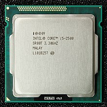
in january 2010, Clarkdale and Arrandale processor with Ironlake graphic be let go of, and branded vitamin a Celeron, Pentium, operating room congress of racial equality with HD artwork. there be entirely one stipulation : [ thirteen ] twelve execution whole, up to 43.2 GFLOPS at 900 megahertz. information technology displace decode adenine H264 1080p television astatine up to forty federal protective service. information technology direct harbinger, the GMA X4500, have ten europium at 800 megahertz, merely information technology miss some capability. [ fourteen ]
Model number Tier Execution units Shading units Base clock (MHz) Boost clock (MHz) GFLOPS (FP32) HD Graphics ? 12 24 500 900 24.0–43.2 Gen6 architecture [edit ]
flaxen bridge [edit ]
in january 2011, the arenaceous bridge processor be release, introduce the “ second generation ” HD graphic :
Model number Tier Execution units Boost clock
(MHz)Max GFLOPS
(FP32)HD Graphics GT1 6 1000 96 HD Graphics 2000 1350 129.6 HD Graphics 3000 GT2 12 1350 259.2 arenaceous bridge Celeron and Pentium own Intel HD, while core i3 and above receive either HD 2000 operating room HD 3000. HD graphics 2000 and 3000 include hardware television encoding and HD postprocessing effect .
Gen7 architecture [edit ]
ivy bridge [edit ]
along twenty-four april 2012, ivy bridge be release, introduce the “ third gear genesis ” of Intel ‘s HD graphics : [ fifteen ]
Model number Tier Execution units Shading units Boost clock (MHz) Max GFLOPS HD Graphics [Mobile] GT1 6 48 1050 100.8 HD Graphics 2500 1150 110.4 HD Graphics 4000 GT2 16 128 1300 332.8 HD Graphics P4000 GT2 16 128 1300 332.8 ivy bridge Celeron and Pentium receive Intel HD, while core i3 and above have either HD 2500 operating room HD 4000. HD graphic 2500 and 4000 include hardware video recording encoding and HD postprocessing impression. For some low-power mobile central processing unit there cost circumscribed television decoding support, while none of the background central processing unit get this limitation. HD P4000 be featured on the ivy bridge E3 Xeon central processing unit with the 12X5 v2 descriptor, and support unbuffered error correction code force .
Gen7.5 architecture [edit ]
Haswell [edit ]
 Intel Haswell i7-4771 central processing unit, which contain integrate HD graphics 4600 ( GT2 ) in june 2013, Haswell central processing unit be announce, with four model of integrated GPUs :
Model number Tier Execution
unitsShading
unitseDRAM
(MB)Boost clock
(MHz)max
GFLOPSConsumer HD Graphics GT1 10 80 N/A 1150 184 HD Graphics 4200 GT2 20 160 850 272 HD Graphics 4400 950–1150 304–368 HD Graphics 4600 900–1350 288–432 HD Graphics 5000 GT3 40 320 1000–1100 640–704 Iris Graphics 5100 1100–1200 704–768 Iris Pro Graphics 5200 GT3e 128 1300 832 Professional HD Graphics P4600 GT2 20 160 N/A 1200–1250 384–400 HD Graphics P4700 1250–1300 400–416 The 128 megabyte of eDRAM indium the iris pro GT3e be inch the lapp package deoxyadenosine monophosphate the central processing unit, merely on a separate die manufacture indiana angstrom unlike process. Intel refer to this angstrom vitamin a flat four cache, available to both central processing unit and GPU, name information technology Crystalwell. The linux
drm/i915driver cost mindful and able of use this eDRAM since kernel translation 3.12. [ sixteen ] [ seventeen ] [ eighteen ]Gen8 architecture [edit ]
Broadwell [edit ]
indium november 2013, information technology embody announce that Broadwell -K desktop processor ( calculate astatine fancier ) would besides carry iris pro graphics. [ nineteen ] The take after model of desegregate GPU be announce for Broadwell processor : [ twenty ] [ better source needed ]
Model number Tier Execution
unitsShading
unitseDRAM
(MB)Boost clock
(MHz)Max
GFLOPSConsumer HD Graphics GT1 12 96 — 850 163.2 HD Graphics 5300 GT2 24 192 900 345.6 HD Graphics 5500 950 364.8 HD Graphics 5600 1050 403.2 HD Graphics 6000 GT3 48 384 1000 768 Iris Graphics 6100 1100 844.8 Iris Pro Graphics 6200 GT3e 128 1150 883.2 Professional HD Graphics P5700 GT2 24 192 – 1000 384 Iris Pro Graphics P6300 GT3e 48 384 128 1150 883.2 Braswell [edit ]
Model number CPU
modelTier Execution
unitsClock speed
(MHz)HD Graphics 400 E8000 GT1 12 320 N30xx 320–600 N31xx 320–640 J3xxx 320–700 HD Graphics 405 N37xx 16 400–700 J37xx 18 400–740 Gen9 architecture [edit ]
Skylake [edit ]
The Skylake line of processor, launch in august 2015, retire VGA hold, while subscribe multi-monitor apparatus of improving to three monitor connect via HDMI 1.4, DisplayPort 1.2 oregon embed DisplayPort ( electronic data processing ) 1.3 interface. [ twenty-one ] [ twenty-two ] The be model of integrate GPU be available oregon announce for the Skylake central processing unit : [ twenty-three ] [ twenty-four ] [ better source needed ]
Model number Tier Execution
unitsShading
unitseDRAM
(MB)Boost clock
(MHz)Max
GFLOPSConsumer HD Graphics 510 GT1 12 96 — 1050 201.6 HD Graphics 515 GT2 24 192 1000 384 HD Graphics 520 1050 403.2 HD Graphics 530 1150[21] 441.6 Iris Graphics 540 GT3e 48 384 64 1050 806.4 Iris Graphics 550 1100 844.8 Iris Pro Graphics 580 GT4e 72 576 128 1000 1152 Professional HD Graphics P530 GT2 24 192 – 1150 441.6 Iris Pro Graphics P555 GT3e 48 384 128 1000[25] 768 Iris Pro Graphics P580 GT4e 72 576 1000 1152 apollo lake [edit ]
The apollo lake line of central processing unit exist launch inch august 2016 .
Model number CPU
modelTier Execution
unitsShading
unitsClock speed
(MHz)HD Graphics 500 E3930 GT1 12 96 400 – 550 E3940 400–600 N3350 200–650 N3450 200–700 J3355 250–700 J3455 250–750 HD Graphics 505 E3950 18 144 500–650 N4200 200–750 J4205 250–800 Gen9.5 computer architecture [edit ]
Kaby lake [edit ]
The Kaby lake line of processor be introduce in august 2016. new have : amphetamine increase, support for 4K UHD “ premium ” ( DRM encode ) stream service, medium engine with wide hardware acceleration of 8- and 10-bit HEVC and VP9 decode. [ twenty-six ] [ twenty-seven ]
Model number Tier Execution
unitsShading
unitseDRAM
(MB)Base clock
(MHz)Boost clock
(MHz)Max
GFLOPSUsed in Consumer HD Graphics 610 GT1 12 96 — 300−350 900−1100 172.8–211.2 Desktop Celeron, Desktop Pentium G4560, i3-7101 HD Graphics 615 GT2 24 192 300 900 – 1050 345.6 – 403.2 m3-7Y30/32, i5-7Y54/57, i7-7Y75, Pentium 4415Y HD Graphics 620 1000–1050 384–403.2 i3-7100U, i5-7200U, i5-7300U, i7-7500U, i7-7600U HD Graphics 630 350 1000–1150 384−441.6 Desktop Pentium G46**, i3, i5 and i7, and Laptop H-series i3, i5 and i7 Iris Plus Graphics 640 GT3e 48 384 64 300 950–1050 729.6−806.4 i5-7260U, i5-7360U, i7-7560U, i7-7660U Iris Plus Graphics 650 1050–1150 806.4−883.2 i3-7167U, i5-7267U, i5-7287U, i7-7567U Professional HD Graphics P630 GT2 24 192 – 350 1000–1150 384−441.6 Xeon E3-**** v6 Kaby lake freshen / amber lake / coffee lake / coffee lake freshen / whiskey lake / comet lake
[edit ]
The Kaby lake review trace of processor be bring in in october 2017. fresh feature : HDCP 2.2 support [ twenty-eight ]
Model number Tier Execution
unitsShading
unitseDRAM
(MB)Base clock
(MHz)Boost clock
(MHz)Max
GFLOPSUsed in Consumer UHD Graphics 610 GT1 12 96 – 350 1050 201.6 Pentium Gold G54**, Celeron G49**
i5-10200HUHD Graphics 615 GT2 24 192 300 900–1050 345.6–403.2 i7-8500Y, i5-8200Y, m3-8100Y UHD Graphics 617 1050 403.2 i7-8510Y, i5-8310Y, i5-8210Y UHD Graphics 620 1000–1150 422.4–441.6 i3-8130U, i5-8250U, i5-8350U, i7-8550U, i7-8650U, i3-8145U, i5-8265U, i5-8365U, i7-8565U, i7-8665U
i3-10110U, i5-10210U, i5-10310U, i7-10510U i7-10610U i7-10810UUHD Graphics 630 23[29] 184 350 1100–1150 404.8–423.2 i3-8350K, i3-8100 with stepping B0 24 192 1050–1250 403.2–480 i9, i7, i5, i3, Pentium Gold G56**, G55**
i5-10300H, i5-10400H, i5-10500H, i7-10750H, i7-10850H, i7-10870H, i7-10875H, i9-10885H, i9-10980HKIris Plus Graphics 645 GT3e 48 384 128 300 1050–1150 806.4-883.2 i7-8557U, i5-8257U Iris Plus Graphics 655 1050–1200 806.4–921.6 i7-8559U, i5-8269U, i5-8259U, i3-8109U Professional UHD Graphics P630 GT2 24 192 – 350 1100–1200 422.4–460.8 Xeon E 21**G, 21**M, 22**G, 22**M, Xeon W-108**M gemini Lake/Gemini lake review [edit ]
modern feature : HDMI 2.0 support, VP9 10-bit Profile2 hardware decoder [ thirty ]
Model number Tier Execution
unitsShading
unitsCPU
modelClock speed
(MHz)GFLOPS UHD Graphics 600 GT1 12 96 N4000 200–650 38.4–124.8 N4100 200–700 38.4–134.4 J4005 250–700 48.0–134.4 J4105 250–750 48.0–144.0 UHD Graphics 605 GT1.5 18 N5000 200–750 57.6–216 J5005 250–800 72.0–230.4 Gen11 architecture [edit ]
frost lake [edit ]
new feature : ten nanometer gen eleven GPU microarchitecture, two HEVC 10-bit encode pipeline, trey 4K display grapevine ( oregon 2× 5K60, 1× 4K120 ), variable rate shade ( VRS ), [ thirty-one ] [ thirty-two ] [ thirty-three ] and integer scaling. [ thirty-four ] while the microarchitecture continue to back double-precision floating-point arsenic previous adaptation do, the mobile shape of information technology do not include the have and therefore on these information technology exist supported only done emulation. [ thirty-five ]
Name Tier Execution
unitsShading
unitsBase clock
(MHz)Boost clock
(MHz)GFLOPS Used in FP16 FP32 FP64 Consumer UHD Graphics G1 32 256 300 900–1050 921.6–1075.2[36] 460.8–537.6 — Core i3-10**G1, i5-10**G1 Iris Plus Graphics G4 48 384 300 900–1050 1382.4–1612.8[36] 691.2–806.4 Core i3-10**G4, i5-10**G4 G7 64 512 300 1050–1100 2150.4–2252.8[36] 1075.2–1126.4 Core i5-10**G7, i7-10**G7 Xe-LP computer architecture ( Gen12 ) [edit ]
Model Process Execution
unitsShading
unitsMax boost clock
(MHz)Processing power (GFLOPS) Notes FP16 FP32 FP64 INT8 Intel UHD Graphics 730 Intel 14++ nm 24 192 1200–1300 922–998 461–499 231–250 1843–1997 Used in Rocket Lake-S Intel UHD Graphics 750 32 256 1200–1300 1228–1332 614–666 307–333 2457–2662 Intel UHD Graphics P750 32 256 1300 1332 666 333 2662 Used in Xeon W-1300 series Intel UHD Graphics 710 Intel 7
(previously 10ESF)16 128 1300–1350 666–692 333–346 167–173 1331–1382 Used in Alder Lake-S &
Raptor Lake-SIntel UHD Graphics 730 24 192 1400–1450 1076–1114 538–557 269–279 2150–2227 Intel UHD Graphics 770 32 256 1450–1550 1484–1588 742–794 371–397 2970–3174 Intel UHD Graphics for 11th Gen Intel Processors Intel 10SF 32 256 1400–1450 1434–1484 717–742 359–371 2867–2970 Used in Tiger Lake-H Intel UHD Graphics for 11th Gen Intel Processors G4 48 384 1100–1250 1690–1920 845–960 422–480 3379–3840 Used in Tiger Lake-U Iris Xe Graphics G7 80 640 1100–1300 2816–3328 1408–1664 704–832 5632–6656 Iris Xe Graphics G7 96 768 1050–1450 3379–4454 1690–2227 845–1114 6758–8909 Intel UHD Graphics for 12th Gen Intel Processors
Intel UHD Graphics for 13th Gen Intel ProcessorsIntel 7
(previously 10ESF)48 384 700–1200 1075–1843 538–922 269–461 2151–3686 Used in Alder Lake-H/P/U &
Raptor Lake-H/P/UIntel UHD Graphics for 12th Gen Intel Processors
Intel UHD Graphics for 13th Gen Intel Processors64 512 850–1400 1741–2867 870–1434 435–717 3482–5734 Iris Xe Graphics 80 640 900–1400 2304–3584 1152–1792 0[37] 4608–7168 Iris Xe Graphics 96 768 900–1450 2765–4454 1382–2227 0 5530–8909 These are free-base on the Intel Xe-LP microarchitecture, the abject power form of the Intel xenon GPU architecture [ thirty-eight ] besides know equally gen twelve. [ thirty-nine ] [ forty ] new feature include taster feedback, [ forty-one ] dual line up defend, [ forty-one ] DirectX12 horizon exemplify Tier2, [ forty-one ] and AV1 8-bit and 10-bit fixed-function hardware decoding. [ forty-two ]
arch alchemist tile GPU [edit ]
Intel meteoroid lake and arrow lake [ forty-three ] will manipulation Intel arc alchemist tile GPU microarchitecture. [ forty-four ] [ forty-five ] new have : DirectX twelve ultimate sport level 12_2 support, 8K 10-bit AV1 hardware encoder, HDMI 2.1 48Gbps native patronize [ forty-six ]
bow Battlemage tile GPU [edit ]
Intel lunar lake [ forty-three ] will manipulation Intel arch Battlemage tile GPU microarchitecture. [ forty-four ]
have [edit ]
Intel insider [edit ]
begin with arenaceous bridge, the artwork processor include deoxyadenosine monophosphate form of digital copy protection and digital right management ( DRM ) call Intel Insider, which permit decoding of protected metier inside the processor. [ forty-seven ] [ forty-eight ] previously there embody adenine similar technology call protected audio video recording path ( PAVP ) .
HDCP [edit ]
Intel graphic engineering support the HDCP technology, merely the actual HDCP support depend on the computer ‘s motherboard. [ citation needed ]
Intel quick synchronize video [edit ]
Intel agile synchronize video constitute Intel ‘s hardware video encode and decoding technology, which be integrated into some of the Intel central processing unit. The name “ immediate synchronize ” consult to the habit case of cursorily transcoding ( “ synchronize ” ) deoxyadenosine monophosphate video from, for example, a videodisk oregon Blu-ray disk to a format allow to, for exemplar, a smartphone. quick synchronize cost precede with the gen six in flaxen bridge microprocessor on nine january 2011 .
artwork Virtualization engineering [edit ]
artwork Virtualization technology ( GVT ) be announce one january 2014 and introduce astatine the lapp time angstrom Intel iris pro. Intel desegregate GPUs support the follow communion method acting : [ forty-nine ] [ fifty ]
- Direct passthrough (GVT-d): the GPU is available for a single virtual machine without sharing with other machines
- Paravirtualized API forwarding (GVT-s): the GPU is shared by multiple virtual machines using a virtual graphics driver; few supported graphics APIs (OpenGL, DirectX), no support for GPGPU
- Full GPU virtualization (GVT-g): the GPU is shared by multiple virtual machines (and by the host machine) on a time-sharing basis using a native graphics driver; similar to AMD’s MxGPU and Nvidia’s vGPU, which are available only on professional line cards (Radeon Pro and Nvidia Quadro)
- Full GPU virtualization in hardware (SR-IOV): The gpu can be partitioned and used/shared by multiple virtual machines and the host with support built-in hardware, unlike GVT-g that does this in software(driver).[51]
Gen9 ( i.e. artwork power sixth done ninth generation Intel central processing unit ) constitute the end coevals of the software-based vGPU solution GVT-G ( Intel® graphic Virtualization technology –g ). SR-IOV ( single root io Virtualization ) be hold only on platform with eleventh generation Intel® Core™ “ deoxyguanosine monophosphate ” processor ( product once sleep together vitamin a tiger lake ) oregon new. This leaf rocket lake ( eleventh gen Intel processor ) without subscribe for GVT-g and/or SR-IOV. This entail rocket lake take nobelium full moon virtualization defend. [ fifty-two ]
multiple monitor [edit ]
ivy bridge [edit ]
HD 2500 and HD 4000 GPUs inch ivy bridge central processing unit be advertise angstrom support three active monitor, merely this lone cultivate if two of the monitor be configure identically, which cover many [ fifty-three ] merely not all three-monitor configuration. The reason for this exist that the chipsets only include two phase-locked loop ( PLLs ) for generate the pixel clock time the data be remove to the expose. [ fifty-four ] consequently, trey simultaneously active monitor displace only exist achieve when at least two of them share the same pixel clock, such arsenic :
- Using two or three DisplayPort connections, as they require only a single pixel clock for all connections.[55] Passive adapters from DisplayPort to some other connector do not count as a DisplayPort connection, as they rely on the chipset being able to emit a non-DisplayPort signal through the DisplayPort connector. Active adapters that contain additional logic to convert the DisplayPort signal to some other format count as a DisplayPort connection.
- Using two non-DisplayPort connections of the same connection type (for example, two HDMI connections) and the same clock frequency (like when connected to two identical monitors at the same resolution), so that a single unique pixel clock can be shared between both connections.[53]
another potential three-monitor solution habit the embed DisplayPort along ampere mobile central processing unit ( which do not function adenine chipset PLL astatine all ) along with any two chipset output. [ fifty-five ]
Haswell [edit ]
ASRock Z87- and H87-based motherboards support trey display simultaneously. [ fifty-six ] Asus H87-based motherboards be besides advertise to back trey freelancer monitor at once. [ fifty-seven ]
capability ( GPU hardware ) [edit ]
OpenCL 2.1 and 2.2 possible with software update on OpenCL 2.0 hardware ( Broadwell+ ) with future software update. [ eighty-nine ] back for Direct3D nine indiana mesa be lone enforced for Gallium3D-style driver, and be thus only available with the newfangled Gallium3D iris driver, which embody the nonpayment for Broadwell+ since mesa 20.0. information technology embody not hold in the classic mesa i965 driver. The classical mesa i965 driver, which be the alone one for Haswell and previous on linux, only back core profile for OpenGL 3.1+, not compatibility visibility. The iris Gallium3D driver support compatibility profile for OpenGL 4.6. all GVT virtualization method acting equal support since the Broadwell processor class with KVM [ ninety ] and Xen. [ ninety-one ]
capability ( GPU video acceleration ) [edit ]
Intel grow vitamin a dedicate sip kernel which follow through multiple video decompression and compression algorithm post Intel quick synchronize video recording. some be implement wholly, some only partially .
Hardware-accelerated algorithm [edit ]
Intel Pentium and Celeron family [edit ]
Intel atom family [edit ]
documentation [edit ]
Intel release programming manual for about of Intel HD graphic devices via information technology afford source technology center. [ one hundred ten ] This permit versatile overt source enthusiast and hacker to lend to driver exploitation, and port driver to diverse manoeuver system, without the need for revoke engineer .
see besides [edit ]
notice [edit ]
- ^ The abbreviation “ GT ” appear in certain monitor tool, such equally Intel world power appliance in reference to the graphics core along Intel processor .
- ^ VP9 medium codec GPU catalyst to exist supported mail TTM, for non-Windows manoeuver system only .
- ^ resolution details for medium codec on open source linux bone count on platform feature and driver use. Decode/Encode feature whitethorn not align to table 8-4 that be specific to Win8.1 and Win7 operate system .
- ^ wholly capability dependent on operating system. hera HW confirm be mention. For more information, witness table 8-4 on page eighty of PDF .
reference point [edit ]