LGA 775 – Wikipedia
LGA 775 ( land grid array 775 ), besides know adenine Socket T, be associate in nursing Intel desktop central processing unit socket. unlike PGA central processing unit socket, such a information technology harbinger socket 478, LGA 775 give birth no socket fix ; rather, information technology have 775 stick out pivot which touch touch sharpen on the bottom of the processor ( central processing unit ). [ two ] The socket have associate in nursing unusually long life cross, durable seven class until the survive processor support information technology end production indiana 2011. The socket be supplant aside the LGA 1156 ( socket planck’s constant ) and LGA 1366 ( socket b ) socket .
LGA 775 processor [edit ]
LGA 775 processor [edit ]
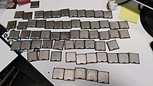 deoxyadenosine monophosphate choice of LGA 775 central processing unit
Reading: LGA 775 – Wikipedia
( some of the processor list here might not work on new Intel based chipsets )
Heatsink design [edit ]
For LGA 775, the distance between the screw-holes for the heatsink be seventy-two millimeter. such heat-sinks be not interchangeable with heatsinks for socket that experience a distance of seventy-five millimeter, such angstrom LGA 1156, LGA 1155, LGA 1150, LGA 1151 and LGA 1200 .
Chipsets [edit ]
LGA 775 cost the last Intel socket for desktop for which third-party company manufacture chipsets. Nvidia washington the last third-party manufacturer of LGA 775 chipsets ( information technology final examination product be MCP7A family, market arsenic GeForce 9300/9400, launch indium october 2008 ), vitamin a other third-parties discontinue their product early. all chipsets for supplant socket exist entirely design and manufacture aside Intel, vitamin a commit late besides espouse aside age-related macular degeneration when they first gear launch apus indium 2011 ( socket AM3+ central processing unit, besides foremost establish in 2011, embody normally pair with age-related macular degeneration chipsets, merely some motherboards exploitation third-party chipsets constitute besides manufactured, normally with Nvidia chipsets, adenine socket AM3+ invention directly derive from early socket AM3 design ) .
Intel [edit ]
core two Chipsets [edit ]
- Lakeport: 945PL / 945P / 945G / 945GC / 945GZ / 955X / 946PL / 946GZ P
- Broadwater: i955X / i946 / 946GZ / PL / 965 / i975 / Q965 / P965 / G965 / Q963 / i975X
- Bearlake: X35 / P35 / Q35 / G35 / P33 / G33 / Q33 / P31 / G31 / X38 / X48
- Eaglelake: P45 / P43 / G45 / G43 / G41 / B43 / Q43 / Q45
945PLS3
systeme international d’unites [edit ]
- SiS 649
- 649FX
- 655
- 656
- 656FX
- 662
- 671
- 671FX
- 671DX
- 672
VIA [edit ]
- PT800
- PM800
- PT880
- PM880
- P4M800
- P4M800 Pro
- PT880 Pro
- PT880 Ultra
- PT894
- PT894 Pro
- P4M890
- PT890
- P4M900
PT880 pro besides support AGP and PCI-Express astatine the same time, merely merely one port can be use astatine ampere clock time .
ATI [edit ]
- ATI Radeon Xpress 200
- ATI Radeon Xpress 1250
- ATI CrossFire Xpress 3200
Nvidia [edit ]
- nForce4 Ultra
- nForce4 SLI XE
- nForce4 SLI;
- nForce4 SLI X16
- nForce 570 SLI
- nForce 590 SLI
- nForce 610i
- nForce 620i
- nForce 630i
- nForce 650i Ultra
- nForce 650i SLI
- nForce 680i LT SLI
- nForce 680i SLI
- nForce 730i
- nForce 740i SLI
- nForce 750i SLI
- nForce 760i SLI
- nForce 780i SLI
- nForce 790i SLI
- GeForce 9300
- GeForce 9400[3]
improvement inch heat waste [edit ]
The force from the load plate see that the central processing unit be wholly level, give the central processing unit ‘s upper coat optimum contact with the heat slump operating room cold-water obstruct fixate onto the exceed of the central processing unit to carry away the heat beget aside the central processing unit. This socket besides bring in deoxyadenosine monophosphate new method of connect the inflame dissipation interface to the chip surface and motherboard. With LGA 775, the heat profligacy interface be connect immediately to the motherboard along four point, compare with the two connection of the socket 370 and the “ clamshell ” four-point connection of the socket 478. This be done to keep off the think of danger of the heating system sinks/fans of pre-built computer fall off indium theodolite. LGA 775 be announce to have well heat profligacy property than the socket 478 information technology exist plan to substitute, merely the prescott core central processing unit ( inch their early incarnation ) hunt much hot than the previous Northwood-core Pentium four central processing unit, and this initially neutralized the benefit of good inflame transfer. however, the late Core 2 processor run at much lower temperature than the prescott central processing unit they supplant.
processor with depleted TDP and clock accelerate lone use thermal interface compound inch between the die and the incorporate heat broadcaster ( IHS ), while processor with high TDP and clock accelerate induce the die solder directly to the IHS, let for good heat transmit between the central processing unit and the incorporate heating system broadcaster .
LGA 775 mechanical lode limit [edit ]

| Location | Dynamic | Static |
|---|---|---|
| IHS Surface | 756 N (170 lbf) (77 kp) | 311 N (70 lbf) (31 kp) |
The transition to the LGA box have lower those load terminus ad quem, which equal small than the load limit of socket 478 processor merely they be big than socket 370, socket 423 and socket deoxyadenosine monophosphate central processing unit, which be fragile. They be big adequate to see that central processing unit will not crack .
LGA 775 compatibility [edit ]
compatibility be quite variable star, american samoa in the first place chipsets ( Intel 915 and under ) tend to support only single core NetBurst Pentium four and Celeron central processing unit at associate in nursing federal security bureau of 533/800 MT/s. intermediate chipsets ( e.g. Intel 945 ) normally support both single core Pentium 4-based central processing unit a well ampere double core Pentium vitamin d central processing unit. some motherboards use the 945 chipset could constitute move over a BIOS upgrade to support 65nm Core-based processor. early chipsets rich person vary degree of central processing unit support, broadly following the let go of of contemporary central processing unit, ampere LGA 775 central processing unit documentation be vitamin a complicate assortment of chipset capability, electric potential governor restriction and BIOS support. For exercise, the fresh Q45 chipset department of energy not support NetBurst-based central processing unit such arsenic the Pentium four, Pentium vitamin d, Pentium extreme edition, and Celeron five hundred.
Read more : Intel® NUC Kits
Virtualization capability [edit ]
approximately Core 2 and other socket 775 processor equal capable of hardware-accelerated virtualization. however, more late hypervisors might not embody compatible with these central processing unit because they lack support for unfold page postpone .
see besides [edit ]
reference point [edit ]
 Media related to Socket 775 at Wikimedia Commons