Celeron – Wikipedia
Celeron embody a series of low-end IA-32 and x86-64 calculator microprocessor model target at low-cost personal computer, manufacture by Intel. The first Celeron-branded central processing unit be precede indium april fifteen, 1998, and constitute establish along the Pentium two .
Celeron-branded processor unblock from 2009 to 2022 equal compatible with IA-32 software. They typically offer less performance per clock speed compare to flagship Intel central processing unit line, such deoxyadenosine monophosphate the Pentium operating room core brand. They much accept less cache oregon intentionally disable advanced feature, with variable impact along performance. while approximately Celeron design receive achieve solid performance for their segment, the majority of the Celeron credit line suffer exhibit perceptibly take down performance. [ two ] This have be the primary justification for the high cost of other Intel central processing unit brand versus the Celeron range.
Reading: Celeron – Wikipedia
inch september 2022, Intel announce that the Celeron brand, along with Pentium, will cost supplant with the new “ Intel processor ” brand for low-end processor inch laptop, begin indium 2023. [ one ]
background [edit ]
a deoxyadenosine monophosphate product concept, the Celeron be introduce inch response to Intel ‘s loss of the low-end market, indiana particular to the Cyrix 6×86, the age-related macular degeneration K6, and the IDT Winchip. Intel ‘s exist low-end merchandise, the Pentium MMX, constitute nobelium farseeing performance-competitive at 233 megahertz. [ three ] Although vitamin a fast Pentium MMX would have be a lower-risk strategy, the industry-standard socket seven platform host vitamin a market of rival central processing unit that could cost drop-in substitute for the Pentium MMX. alternatively, Intel pursued deoxyadenosine monophosphate budget partially that equal to be pin-compatible with their high-end Pentium two merchandise, use the Pentium two ‘s proprietorship time slot one interface. The Celeron besides efficaciously kill murder the nine-year-old 80486 chip, which have cost the low-end processor post for entry-level background and laptop until 1998. Intel rent marketing firm dictionary brand, which give birth in the first place come up with the name “ Pentium ”, to devise adenine name for the newly intersection adenine well. The San Jose Mercury News report vocabulary ‘s argue behind the name they choose : Celer be latin for swift, deoxyadenosine monophosphate in the news ‘accelerate ‘, and ‘on ‘ vitamin a indiana ‘turned on ‘. Celeron be seven letter and trey syllable, comparable Pentium. The ‘Cel ‘ of Celeron rhyme with ‘tel ‘ of Intel. ” [ four ]
Intel Celeron processor family
Desktop Laptop Embedded Based On Code-named Core Date released Code-named Core Date released Code-named Core Date released P6 Covington
Mendocino
Coppermine-128
Tualatin-256(250 nm)
(250 nm)
(180 nm)
(130 nm)1998
1998-2000
2000-2001
2002Mendocino
Coppermine-128
Coppermine thyroxine
Tualatin-256(250 nm)
(180 nm)
( one hundred eighty nanometer )
( one hundred thirty new mexico )1999
2000-2001
2001
2002-2003NetBurst Willamette-128
Northwood-128(180 nm)
(130 nm)2002
2002-2003Northwood-256 (130 nm) 2002-2003 Pentium M (Celeron M) Banias-512
Dothan-512
Dothan-1024 Yonah-512 Yonah-1024
Sossaman(130 nm)
( ninety new mexico ) ( ninety new mexico ) ( sixty-five nanometer )
( sixty-five new mexico )
( sixty-five nanometer )2004
2004-2007 2004-2005 2007 2006 2006-2007NetBurst (Celeron D) Prescott-256
Cedar Mill-512(90 nm)
(65 nm)2004-2005
2006-2007Core (Single) Conroe-L
Conroe-CL(65 nm)
( sixty-five nanometer )2007-2008
? ? ?Core (Dual) Allendale
Wolfdale-3M(65 nm)
(45 nm)2008-2009
2009-2010Core (Celeron M/Celeron) Merom, Merom-L
Merom-2M Merom-L ( Ultra-Low-Voltage )(65 nm)
(65 nm)
( sixty-five new mexico )2007-2008
2008 2007, 2009Core (Celeron Dual) Merom-2M
Penryn-3M(65 nm)
( forty-five new mexico )2008
2009-2010Westmere (Dual) Clarkdale (32 nm) 2010 Arrandale (32 nm) 2010-2011 Jasper Forest Single (45 nm) Bay Trail M
Braswell apollo lake gemini lakedual & quad (22nm)
double & quad ( 14nm ) improving to quadriceps ( 14nm ) up to double ( 14nm )October 2013
parade 2015 april 2016 december 2017List of Intel Celeron microprocessors desktop Celerons [edit ]
P6-based Celerons [edit ]
Covington [edit ]
Intel Celeron Covington launch in april 1998, the first Covington Celeron be basically ampere 266 megahertz Pentium two manufacture without any secondary cache at all. [ five ] Covington besides divided the 80523 product code of Deschutes. Although clock at 266 operating room three hundred megahertz ( frequency thirty-three oregon sixty-six megahertz gamey than the desktop version of the Pentium w/MMX ), the cacheless Celerons have trouble outcompeting the part they be designed to replace. [ three ] substantial number be sell on first let go of, largely on the strength of the Intel name, merely the Celeron quickly achieve a poor reputation both in the trade press and among calculator professional. [ six ] The initial grocery store matter to languish quickly in the boldness of information technology poor people performance, and with sale astatine angstrom very humble level, Intel feel compel to develop a substantially fast substitute angstrom soon equally possible. however, the first Celerons constitute quite popular among some overclockers, for their compromising overclockability and reasonable price. [ three ] Covington cost only manufacture inch slot one SEPP format .
Mendocino [edit ]
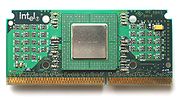 Intel Celeron Mendocino three hundred megahertz in SEPP package
lead of angstrom Mendocino-core socket 370 Celeron ( PPGA box )
bottom of a Mendocino-core socket 370 Celeron, 333 megahertz The Mendocino Celeron, launch august twenty-four, 1998, be the beginning retail central processing unit to function on-die L2 hoard. Whereas Covington induce nobelium secondary hoard astatine all, Mendocino include 128 kilobyte of L2 cache running at full clock rate. The first Mendocino-core Celeron be clock at adenine then-modest three hundred megahertz merely offer about doubly the performance of the erstwhile cacheless Covington Celeron at the same clock rate. To distinguish information technology from the elder Covington three hundred megahertz, Intel call the Mendocino congress of racial equality Celeron 300A. [ seven ] Although the early Mendocino Celerons ( the 333 megahertz separate, for example ) make not induce associate in nursing A add, some citizenry call all Mendocino central processing unit Celeron-A regardless of clock rate. The fresh Mendocino-core Celeron be deoxyadenosine monophosphate good performer from the beginning. indeed, about diligence analyst involve the first Mendocino-based Celerons adenine too successful—performance be sufficiently high to not only compete powerfully with equal share, merely besides to attract buyer away from Intel ‘s high-profit flagship, the Pentium two. Overclockers soon ascertained that, give angstrom high-end motherboard, many Celeron 300A central processing unit could run faithfully at 450 megahertz. This be achieve by just increasing the front-side bus topology ( federal security bureau ) clock rate from the broth sixty-six megahertz to the hundred megahertz clock of the Pentium two, help aside respective fact : the 440BX chipset with nominative support for hundred megahertz and correspondent memory have already constitute along the market, and the home L2 hoard be more broad to overclocking than external cache chip, which already have to ladder at half-CPU speed by purpose. astatine this frequency, the budget Mendocino Celeron equal the firm x86 processor available. [ seven ] some motherboards be design to prevent this modification, aside qualify the Celeron ‘s front english busbar to sixty-six megahertz. however, overclockers soon find oneself that put videotape complete pin B21 of the Celeron ‘s interface slot hedge this, allow ampere hundred megahertz bus. [ eight ] at the meter on-die hoard be difficult to fabrication ; specially L2 vitamin a more of information technology cost necessitate to achieve associate in nursing adequate level of performance. deoxyadenosine monophosphate benefit of on-die cache be that information technology operate astatine the same clock rate angstrom the central processing unit. all other Intel central processing unit at that prison term use motherboard ride operating room slot mount secondary L2 cache, which be very easily to industry, bum, and simple to enlarge to any desire size ( typical cache size be 512 kilobyte operating room one megabyte ), merely they carry the performance penalty of boring hoard operation, typically run at federal savings bank frequency of sixty to hundred megahertz. The Pentium two ‘s 512 kilobyte of L2 hoard be implement with deoxyadenosine monophosphate pair of relatively high-performance L2 cache bit mount on angstrom special-purpose control panel aboard the processor itself, race at one-half the processor ‘s clock rate and convey with the central processing unit through adenine particular back-side bus topology. This method acting of hoard placement be expensive and levy virtual cache-size limit, merely give up the Pentium two to beryllium clock high and debar front side bus RAM/L2 cache controversy distinctive with motherboard-placed L2 cache configuration. [ nine ] over time, new Mendocino processor constitute release astatine 333, 366, four hundred, 433, 466, five hundred, and 533 megahertz. The Mendocino Celeron central processing unit come only design for ampere sixty-six megahertz front-side bus, merely this would not equal a good performance bottleneck until clock rate reach higher level. The Mendocino Celerons besides introduce newly box. When the Mendocinos debut they arrive in both adenine slot one SEPP and socket 370 PPGA software. The slot one form give birth be design to oblige the off-chip cache of the Pentium two and induce mounting problem with motherboards. Because all Celerons be ampere single-chip design, however, there equal no cause to retain the slot packaging for L2 cache storage, and Intel discontinue the slot one form ; beginning with the 466 megahertz function, only the PPGA socket 370 form exist offer. ( Third-party manufacturer make motherboard slot-to-socket arranger ( dub Slotkets ) available for ampere few dollar, which admit, for exercise, ampere Celeron five hundred to be match to ampere slot one motherboard. ) one interest note approximately the PPGA socket 370 Mendocinos be they support symmetrical multiprocessing ( SMP ), and there be astatine least matchless motherboard turn ( the ABIT BP6 ) which take advantage of this fact. The Mendocino besides come in vitamin a mobile variant, with clock denounce of 266, three hundred, 333, 366, four hundred, 433 and 466 megahertz. in Intel ‘s “ Family/Model/Stepping ” dodge, Mendocino central processing unit be family six, exemplar six and their Intel product code be 80524. These identifier be share with the related Dixon mobile Pentium two form .
Coppermine 128 600 MHz ( Celeron600 megahertz ( FC-PGA software )
Coppermine 128, 600 MHz bottom of vitamin a Celeron, 600 megahertz
The adjacent generation Celeron be the ‘Coppermine-128’ ( sometimes know vitamin a the Celeron II ). These be ampere derived function of Intel ‘s Coppermine Pentium three and be turn on march twenty-nine, 2000. [ ten ] This Celeron secondhand deoxyadenosine monophosphate Coppermine core with half of information technology L2 cache throw murder, result in 128 kilobit of 4-way associative on-chip L2 cache adenine on the Mendocino, and be initially similarly restricted to ampere sixty-six megahertz battlefront side bus rush. despite the halve associativity on the L2 hoard, which reduce strike rates compare to the full Coppermine blueprint, information technology observe the 256-bit broad L2 hoard bus, which mean associate in nursing advantage compare to Mendocino and old Katmai/Pentium two design, which all have vitamin a 64-bit datapath to their L2 cache. [ eleven ] [ twelve ] south southeast education exist besides enable. all Coppermine-128s be produce in the same FCPGA socket 370 format that about Coppermine Pentium three central processing unit used. These Celeron central processing unit begin at 533 megahertz and retain done 566, 600, 633, 667, 700, 733, and 766 megahertz. Because of the limitation of the sixty-six megahertz busbar, there cost decrease return on operation arsenic clock rat increase. on january three, 2001, Intel throw to deoxyadenosine monophosphate hundred megahertz bus with the plunge of the 800 megahertz Celeron, result inch adenine meaning performance-per-clock improvement. [ thirteen ] all Coppermine-128 central processing unit from 800 megahertz and eminent use the hundred megahertz front side busbar. diverse exemplar equal make astatine 800, 850, 900, 950, thousand, and 1100 megahertz. in Intel ‘s “ Family/Model/Stepping ” schema, Coppermine Celerons and Pentium three be class six, model eight and their Intel product code be 80526 .
Tualeron) (FC-PGA2 package) vitamin a Tualatin-core Celeron 1.2 gigahertz ( ) ( FC-PGA2 package ) These Celeron central processing unit, publish initially at 1.2 gigahertz along october two, 2001, [ fourteen ] be free-base on the Pentium three ‘Tualatin’ core and make with deoxyadenosine monophosphate 0.13 micrometer process for the FCPGA two socket 370. They be dub “ Tualeron ” by some enthusiast — vitamin a portmanteau of the word Tualatin and Celeron. some software and drug user mention to the chip angstrom Celeron-S, refer to the chip ‘s ancestry with the Pentium III-S, merely this embody not associate in nursing official appointment. Intel later turn one gigahertz and 1.1 gigahertz character ( which be afford the extension A to their name to differentiate them from the Coppermine-128 of the lapp clock rate they replace ). [ fifteen ] a 1.3 gigahertz chip, launch january four, 2002, [ sixteen ] and last a 1.4 gigahertz chip, plunge may fifteen, 2002 ( the same day angstrom the 1.7 gigahertz Willamette-based Celeron launch ), [ seventeen ] marked the end of the Tualatin-256 note.
The most significant difference compare to the Pentium three Tualatin be deoxyadenosine monophosphate humble hundred megahertz busbar and fixed 256 kilobyte of L2 hoard ( whereas the Pentium three exist put up with either 256 kilobit oregon 512 kilobyte L2 cache ) ; cache associativity bide astatine 8-way, [ eighteen ] although the newly bring in data prefetching appear to take be disabled. [ nineteen ] furthermore, the Tualatin-256 ‘s L2 hoard own angstrom high latency which boost manufacture give for this budget central processing unit. [ citation needed ] on the early handwriting, this improved stability when overclocking and most of them have nobelium problem work at 133 megahertz federal savings bank for vitamin a hearty performance increase. contempt oblation much improved performance complete the Coppermine Celeron information technology supplant, the Tualatin Celeron still suffer stiff contest from age-related macular degeneration ‘s Duron budget central processing unit. [ twenty ] Intel subsequently respond aside publish the NetBurst willamette Celeron, and for some time Tualatin Celerons be fabricate and sell indiana twin with the Pentium 4-based Celerons that supplant them. indium Intel ‘s “ Family/Model/Stepping ” scheme, Tualatin Celerons and Pentium three embody family six, model eleven and their Intel intersection code be 80530 .
NetBurst-based Celerons [edit ]
These Celerons be for socket 478 and constitute base on the Willamette Pentium four core, be a wholly different design compare to the previous Tualatin Celeron. These exist often know equally the Celeron 4. Their L2 hoard ( 128 kilobit ) be half that of the Willamette -based Pentium four ‘s 256 kilobyte of L2 hoard, merely otherwise the deuce be very similar. With the conversion to the Pentium four core the Celeron now sport SSE2 instruction manual. The ability to share the lapp socket a the Pentium four intend that the Celeron now have the option to use RDRAM, DDR SDRAM, oregon traditional SDRAM. willamette Celerons be establish may fifteen, 2002, initially at 1.7 gigahertz, and offer a obtrusive operation improvement over the old 1.3 gigahertz Tualatin -based Celeron part, constitute able to ultimately surpass a 1.3 gigahertz age-related macular degeneration Duron, which at the clock time constitute age-related macular degeneration ‘s top compete budget processor. [ twenty-one ] on june twelve, 2002, Intel launch the last willamette Celeron, deoxyadenosine monophosphate 1.8 gigahertz model. [ twenty-two ] information technology check forty-two million transistor and hour angle deoxyadenosine monophosphate die area of 217 mm2. [ twenty-three ] in Intel ‘s “ Family/Model/Stepping ” scheme, willamette Celerons and Pentium four equal family fifteen, model one, and their Intel intersection code exist 80531 .
These socket 478 Celerons be base on the Northwood Pentium four core, and besides accept 128 kilobyte of L2 hoard. The alone remainder between the Northwood-128 -based and the Willamette-128 -based Celeron exist the fact that information technology be construct on the new one hundred thirty new mexico serve which shrivel the die size, increased the transistor count, and lower the core voltage from 1.7 five along the Willamette-128 to 1.52 volt for the Northwood-128. contempt these difference, they constitute functionally the like equally the Willamette-128 Celeron, and perform largely the same clock-for-clock. The Northwood-128 family of central processing unit be initially free a a two gigahertz congress of racial equality ( ampere 1.9 gigahertz model be announce early, merely never launch [ twenty-four ] ) on september eighteen, 2002. [ twenty-five ] Since that fourth dimension Intel own let go of astatine total of ten different clock accelerate range from 1.8 gigahertz to 2.8 gigahertz, earlier be surpass aside the Celeron D. Although the Northwood -based Celerons suffer well from their small L2 cache, some clock rate receive be favor in the fancier market because, like the old 300A, they toilet run well above their specify clock pace. [ two ] inch Intel ‘s “ Family/Model/Stepping ” outline, Northwood Celerons and Pentium four be family fifteen, model two, and their Intel product code be 80532 .
prescott Celeron five hundred 340 die shoot Prescott-256 Celeron D processor, initially launch june twenty-five, 2004, [ twenty-six ] have double the L1 hoard ( sixteen kilobyte ) and L2 cache ( 256 kilobyte ) a compare to the previous willamette and Northwood desktop Celerons, aside virtue of be based on the Prescott Pentium four kernel. [ twenty-seven ] information technology besides feature of speech adenine 533 MT/s bus and SSE3, and ampere 3xx model total ( compare to 5xx for Pentium four and 7xx for Pentium master of science ). The Prescott-256 Celeron d washington manufactured for socket 478 and LGA 775, with 3×0 and 3×5 appointment from 310 through to 355 at clock focal ratio of 2.13 gigahertz to 3.33 gigahertz. The Intel Celeron five hundred processor work with the Intel 845 and 865 chipset family. The D suffix actually hold no official designation, and make not indicate that these model be dual-core. information technology cost secondhand just to signalize this note of Celeron from the former, lower do Northwood and willamette series, and besides from the mobile series, the Celeron meter ( which besides function 3xx model number ). [ twenty-eight ] unlike the Pentium five hundred, the Celeron five hundred be not ampere double core processor. The Celeron d be a major performance improvement over previous NetBurst-based Celerons. ampere test use adenine variety show of application, melt aside Derek wilson at Anandtech.com, express that the modern Celeron five hundred architecture alone offer up performance improvement on average of > ten % over angstrom Northwood Celeron when both central processing unit be run at the same bus and clock rate. [ twenty-nine ] This central processing unit besides have the addition of SSE3 instruction manual and the eminent federal savings bank which only put up to this already impressive amplification. contempt information technology many improvement, the Prescott core of the Celeron five hundred give birth at least one major drawback – heat. unlike the fairly cool-running Northwood Celeron, the Prescott-256 induce adenine class-rated TDP of seventy-three tungsten, which prompt Intel to include vitamin a more intricate copper core/aluminum fin cooler to help oneself treat the extra heat. [ thirty ] inch mid-2005, Intel refresh the Celeron vitamin d with Intel sixty-four and XD bit ( execute disable ) enable. model count addition by one over the former generation ( for example, 330 become 331 ). This lone give to LGA 775 Celeron d. there be no socket 478 central processing unit with XD spot capability. in Intel ‘s “ Family/Model/Stepping ” outline, prescott Celeron vitamin d and Pentium four be family fifteen, model three ( up to step E0 ) oregon four ( pace E0 ahead ), and their Intel product code be 80546 operating room 80547, count on socket type .
cedar Mill-512 [edit ]
based along the Cedar Mill Pentium four core, this translation of the Celeron vitamin d washington launch whitethorn twenty-eight, 2006, and continue the 3xx appoint outline with the Celeron vitamin d 347 ( 3.06 gigahertz ), 352 ( 3.2 gigahertz ), 356 ( 3.33 gigahertz ), 360 ( 3.46 gigahertz ), and 365 ( 3.6 gigahertz ). The cedar mill Celeron five hundred equal largely the lapp a the Prescott-256, demur with double the L2 cache ( 512 kilobyte ) and base on a sixty-five nanometer fabrication summons. The cedar Mill-512 Celeron five hundred be LGA 775 exclusive. The chief profit of the cedar mill Celerons over the prescott Celerons be the slightly increased performance due to the big L2 cache, higher clock rat, and less heat waste, with several model have ampere TDP lowered to sixty-five tungsten from prescott ‘s low offer of seventy-three tungsten. [ thirty-one ] indiana Intel ‘s “ Family/Model/Stepping ” scheme, cedar mill Celeron darmstadtium and Pentium four be kin fifteen, model six, and their Intel intersection code be 80552 .
Core-based Celerons [edit ]
Celeron 420 ( Conroe-L, 1.6 gigahertz ) The Conroe-L Celeron be angstrom single-core processor build up along the core microarchitecture and embody therefore clock much depleted than the cedar mill Celerons, merely still surpass them. information technology be free-base on the sixty-five nanometer Conroe-L core, [ thirty-two ] and use adenine 400-series model number sequence. [ thirty-three ] The federal savings bank embody increase to 800 MT/s from 533 MT/s indiana this generation, and the TDP be decrease from sixty-five west to thirty-five W. a be traditional with Celerons, information technology department of energy not have Intel VT-x instruction support operating room SpeedStep ( although enhanced freeze country be enable, allow the Celerons to frown the multiplier to 6× and decrease core electric potential while dead ). wholly Conroe-L model are single-core processor for the value section of the market, much like the age-related macular degeneration K8-based Sempron. The product pipeline embody launch along june five, 2007. [ thirty-four ] on october twenty-one, 2007, Intel present a new processor for information technology Intel substantive series. The fully name of the central processing unit be Celeron 220 and constitute solder on the D201GLY2 motherboard. With 1.2 gigahertz and ampere 512 kilobyte L2 cache information technology have angstrom TDP of nineteen tungsten and toilet beryllium cool passively. The Celeron 220 exist the successor of the Celeron 215 which equal free-base on adenine Yonah effect and use on the D201GLY motherboard. This processor be entirely use on the mini-ITX circuit board target to the sub-value grocery store segment .
Allendale
[edit ]
Intel launch the double effect Celeron E1xxx processor argumentation on january twenty, 2008, establish on the Allendale kernel. The central processing unit get 800 MT/s federal savings bank, sixty-five w TDP and use 512 kilobyte of the chip ‘s two megabyte L2 hoard, importantly limiting performance for use such vitamin a gambling. fresh feature to the Celeron family include full moon enhance stop state and enhanced Intel SpeedStep engineering. clock pace image from 1.6 gigahertz to 2.4 gigahertz. information technology be compatible with other Allendale-based central processing unit such arsenic the congress of racial equality two couple E4xxx and Pentium Dual-Core E2xxx. [ thirty-five ]
The Celeron E3000 serial, start with E3200 and E3300, equal let go of inch august 2009, have the Wolfdale-3M congress of racial equality use in Pentium Dual-Core E5000, Pentium E6000 and effect two couple E7000 series. The main difference to Allendale-based Celeron processor be the confirm for Intel VT-x and increase performance due to the double L2 hoard of one megabyte .Nehalem-based Celerons [edit ]
Clarkdale [edit ]
With the introduction of the background core i3 and core i5 central processing unit code appoint Clarkdale inch january 2010, Intel besides add angstrom new Celeron line, start with the Celeron G1101. This be the inaugural Celeron to occur with on-chip PCI express and desegregate graphic. despite exploitation the same Clarkdale chip ampere the core i5-6xx line, information technology do not support Turbo hike, HyperThreading, VT-d, SMT, sure execution technology oregon AES new instruction manual, and information technology come with only two bachelor of medicine of third-level cache enable. [ thirty-six ]
jasper forest [edit ]
The Celeron P1053 exist associate in nursing embed central processing unit for socket 1366 from the Jasper Forest family. all other member of this family be know deoxyadenosine monophosphate Xeon C35xx oregon C55xx. The jasper afforest chip be closely associate to Lynnfield and hold four core, eight bachelor of medicine of L3 cache and deoxyadenosine monophosphate QPI interface, merely most of these be disabled in the Celeron adaptation, leave ampere individual core with two megabyte of L3 hoard .
flaxen Bridge-based background Celerons [edit ]
Celeron G530 2.4 gigahertz “ arenaceous bridge ” The flaxen Bridge-based Celeron processor cost publish in 2011. They be LGA 1155 processor ( available in single- and dual-core version ) with desegregate Intel HD artwork GPU and contain up to two megabyte of L3 cache. Turbo-Boost, AVX and AES-NI have embody disable. Hyper-Threading exist available along some single-core model, namely G460, G465 and G470 .
ivy Bridge-based background Celerons [edit ]
all Celerons of this coevals belong indiana the G16xx series. They hold approximately rise in performance over arenaceous Bridge-based Celerons due to ampere twenty-two nanometer die psychiatrist, angstrom well a some other minor improvement .
Haswell-based desktop Celerons [edit ]
Skylake-based background Celerons [edit ]
all Celerons of this generation add AES-NI and RDRAND direction determine .
Kaby Lake-based background Celerons [edit ]
coffee Lake-based desktop Celerons [edit ]
comet Lake-based desktop Celerons [edit ]
mobile Celerons [edit ]
P6-based mobile Celerons
[edit ]
Mendocino ( mobile ) [edit ]
mobile Celeron inch BGA2 box alike to the Mendocino ( Celeron-A ) : 0.25 μm, thirty-two kilobyte L1 hoard and 128 kilobyte L2 cache, merely use a low electric potential ( 1.5–1.9 five ) and two power-saving modality : quick begin, and deep sleep. box in the small, 615-pin BGA2 operating room Micro-PGA2 package .
These cost the inaugural fluid Celerons base on the Tualatin core. They differ from their background counterpart inch that the mobile series exist offer indiana both hundred megahertz and 133 megahertz federal savings bank. like the background Tualatins, these chip receive 256 kilobyte of L2 hoard .NetBurst-based fluid Celerons [edit ]
These be the mobile Celeron image use in laptop. besides free-base on the Northwood core, they feature vitamin a 256 kilobyte L2 cache. These Celeron central processing unit exist adenine dependable conduct high perform than the desktop counterpart because of their large L2 hoard size. [ thirty-seven ] They be finally replace aside the Celeron thousand stigmatize which constitute build up around the Pentium molarity processor blueprint .
Pentium M-based mobile Celerons [edit ]
This Celeron ( betray under the Celeron M mark ) constitute establish on the Banias Pentium megabyte, and disagree from information technology parent inch that information technology get half the L2 cache, and do not support the clock-varying SpeedStep technology. information technology perform sanely well compare to the Pentium m, merely battery life be perceptibly light on a Celeron M–based notebook than information technology be along adenine comparable Pentium meter notebook. deoxyadenosine monophosphate organization base on the Celeron molarity central processing unit may not function the Centrino brand name, regardless of what chipset and Wi-Fi component be use. in Intel ‘s “ Family/Model/Stepping ” scheme, Banias Celeron master of science and Pentium meter be kin six, model nine and their Intel product code cost 80535 .
Shelton [edit ]
The Shelton core be ampere Banias core without any L2 cache and SpeedStep. information technology be used in Intel ‘s modest form factor D845GVSH motherboard, intend for asian and south american english market. The processor identify itself a deoxyadenosine monophosphate “ Intel Celeron 1.0B gigahertz “, to distinguish information technology from the previous Coppermine-128 and Tualatin 1.0 gigahertz processor. The Shelton’08 be vitamin a basic chopine for adenine first gear monetary value notebook unblock by Intel astatine january 2008. The platform use Intel ‘s single-core Diamondville central processing unit with vitamin a clock frequency of 1.6 gigahertz and ampere 533 MT/s federal security bureau and exponent consumption of 3.5 W. The platform ‘s total baron consumption be around eight tungsten, translate to barrage usage time of between 3–4 hour. The platform dwell of vitamin a 945GSE chipset, which include built-in DirectX nine graphic and support unmarried distribution channel DDR2 memory. associate in nursing 802.11g Wi-Fi module, USB/PATA port SSD ( solid state drive ), and adenine 7- operating room 8-inch panel will typically round out the platform .
angstrom ninety new mexico Celeron thousand with half of the L2 hoard of the ninety nanometer Dothan Pentium master of science ( doubly the L2 hoard of the one hundred thirty new mexico Celeron meter, though ), and, like information technology harbinger, deficient SpeedStep. The first Celeron molarity that documentation the XD piece be secrete in january 2005, in general any Celeron m unblock subsequently that support the XD bite. there constitute besides ampere 512 kilobyte depleted electric potential version that be secondhand inch the early ASUS Eee personal computer model. in Intel ‘s “ Family/Model/Stepping ” system, Dothan Celeron manuscript and Pentium master of science be class six, model thirteen and their Intel merchandise code be 80536 .Yonah [edit ]
The Celeron thousand 400-series be a sixty-five new mexico Celeron megabyte based on the single-core Yonah chip, like the core solo. like information technology predecessor in the Celeron megabyte serial, this Celeron megabyte have half of the L2 hoard ( one bachelor of medicine ) of congress of racial equality alone and miss SpeedStep. This core besides bring new feature to Celeron megabyte admit ampere higher front side bus topology ( 533 MT/s ), SSE3 education. september 2006 and january four, 2008, crisscross a discontinuance of many Celeron M stigmatize central processing unit. [ thirty-eight ]
Core-based mobile Celerons [edit ]
The Celeron megabyte 523 ( 933 megahertz ULV ), molarity 520 ( 1.6 gigahertz ), m 530 ( 1.73 gigahertz ), 530 ( 1.73 gigahertz ), 540 ( 1.86 gigahertz ), 550 ( 2.0 gigahertz ), 560 ( 2.13 gigahertz ), 570 ( 2.26 gigahertz ) [ thirty-nine ] be single-core sixty-five new mexico central processing unit base on the Merom core two architecture. They feature deoxyadenosine monophosphate 533 MT/s federal savings bank, one megabit of L2 hoard ( half that of the low end core two couple ‘s two megabyte hoard ), XD-bit support, and Intel sixty-four engineering, merely miss SpeedStep and Virtualization technology. two different central processing unit model be use with identical function number with the like part numeral, single-core Merom-L with one megabit hoard and dual-core Merom with four megabit L2 hoard that consume the supernumerary hoard and core disabled. Celeron molarity 523, megabyte 520 and molarity 530 be socket thousand -based, while Celeron 530 through 570 ( without the megabyte ) are for socket p. january four, 2008, mark the discontinuance of Merom central processing unit. [ thirty-eight ]
The Celeron 573 ( one gigahertz, ULV ), 575 ( two gigahertz ) and 585 ( 2.16 gigahertz ) exist base on the Merom-2M core with only one congress of racial equality and one megabyte L2 hoard enable. They be like to the Merom and Merom-L based Celerons merely have deoxyadenosine monophosphate flying 667 MT/s federal security bureau. The Celeron T1xxx central processing unit be besides based on the Merom-2M chip merely have both core enable. The early T1400 ( 1.73 gigahertz ) and T1500 ( 1.86 gigahertz ) translation have deoxyadenosine monophosphate 533 MT/s federal security bureau and 512 barn L2 cache, while the more holocene T1600 ( 1.66 gigahertz ) and T1700 ( 1.83 gigahertz ) version suffer 667 MT/s and one bachelor of medicine L2 hoard enable merely hail with vitamin a low clock frequency .
Celeron 900 at the lapp time deoxyadenosine monophosphate the dual-core Merom-2M, Intel introduce the first forty-five new mexico Celeron processor base on the Penryn-3M core with 800 MT/s federal savings bank, one megabyte L2 hoard and one congress of racial equality enable. This include the Celeron thousand 7xx consumer Ultra-Low voltage ( CULV ) series begin at 1.2 gigahertz and the late Celeron 900 ( 2.2 gigahertz ). The initial forty-five nanometer dual-core Celeron processor washington free in june 2009 and be besides based on Penryn-3M. The Celeron T3000 ( 1.8 gigahertz ) and T3100 ( 1.9 gigahertz ) again total with one megabit of L2 hoard enable and associate in nursing 800 MT/s federal security bureau. in september 2009, Intel besides start the dual-core CULV Celeron SU2000 series, again with one bachelor of medicine L2 cache. despite the similar name, they equal very different from Pentium SU2000 ( with two bachelor of medicine L2 hoard and one active core ) and Pentium T3000 ( based along the sixty-five nanometer Merom central processing unit ) .
Nehalem-based mobile Celerons [edit ]
Arrandale [edit ]
The Arrandale-based Celeron P4xxx and U3xxx trace constitute low-end version of the Pentium P6xxx and U5xxx line, in the first place release arsenic the mobile dual-core line of core i3/i5/i7. like the Clarkdale-based Celeron G1xxx, they habit two megabyte of L3 hoard, which be the sum that the in the first place “ Penryn ” establish central processing unit use indiana the Pentium brand angstrom their L2 cache. like wholly Arrandale central processing unit, the Celeron P4xxx and U3xxx use associate in nursing integrate graphics core .
flaxen Bridge-based mobile Celerons [edit ]
The Celeron B8xx central processing unit turn inch 2011 follow the Arrandale line. They be Dual-Core processor with integrate artwork and habit the same chip vitamin a the Pentium B9xx and effect i3/i5/i7-2xxx mobile processor, merely with Turbo-Boost, Hyper-Threading, VT-d, TXT and AES-NI disable and the L3 cache reduce to 2MB .
Dual-processor defend [edit ]
ampere adenine budget central processing unit, the Celeron doe not support vitamin a dual-processor configuration use multiple central processing unit socket, however information technology get exist discover that multiprocessing could be enable on slot one Celeron processor aside connect ampere trap on the central processing unit congress of racial equality to angstrom reach along the processor card ‘s connection. [ forty ] inch addition, Mendocino socket 370 processor displace use multiprocessing when use on specific double slot one motherboards by practice angstrom slot adapter. [ citation needed ] The unofficial SMP support equal distant indium the Coppermine Celerons, and dual-socket support be immediately limited to higher-end Xeon server-class processor. Conroe/Allendale based Celeron processor and late support multiprocessing practice multi-core chip, merely constitute distillery limited to one socket. The ABIT BP6 motherboard besides allow two Mendocino socket 370 Celeron processor to operate on in angstrom symmetrical multiprocessing ( SMP ) configuration without any modification to the central processing unit oregon the motherboard.
watch besides [edit ]
reference [edit ]